
Renewable energy systems increasingly depend on electronic assemblies for power conversion, monitoring, communication, control, sensing, protection, and energy management.
Depending on the product architecture, PCB assemblies can be found in applications such as:
- Solar inverters
- Solar power control electronics
- Energy storage systems
- Battery management electronics
- Wind power control systems
- Power conversion equipment
- Energy monitoring systems
- EV charging equipment
- Industrial energy-management systems
These products can create demanding manufacturing requirements because control electronics and power electronics may exist within the same product platform.
Some PCBAs are dominated by small SMT components, while others combine SMT devices with transformers, inductors, relays, terminal blocks, connectors, large capacitors, and other through-hole components.
As a result, a complete PCB assembly solution for renewable energy applications may require:
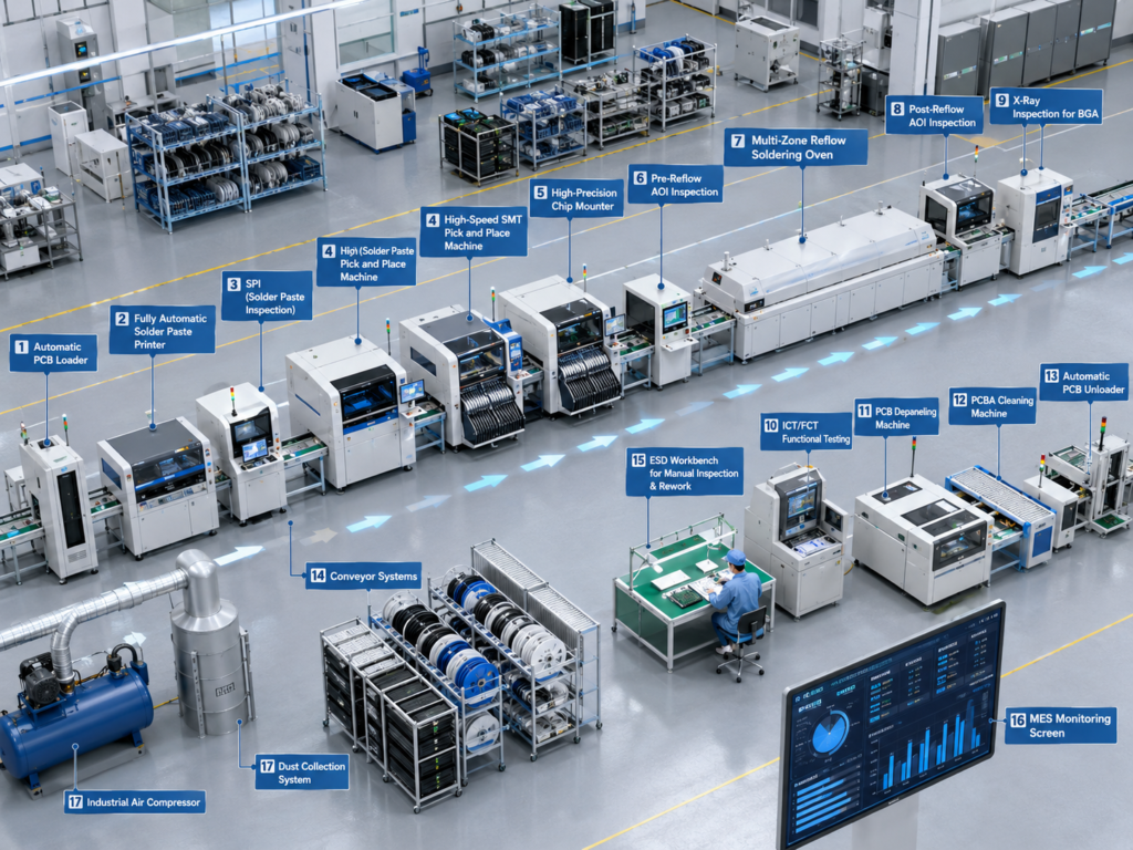
Solder Paste Printing → SPI → SMT Placement → Reflow → AOI → THT Assembly → Wave/Selective Soldering → Inspection → Testing
Depending on the product and operating environment, additional processes can include cleaning, conformal coating, traceability, and final functional testing.
The correct production line should be designed around the actual PCB, BOM, production capacity, product mix, quality requirements, and factory layout.
Renewable Energy Electronics Are Not One Product Category
One of the most important points when planning a renewable energy PCBA line is that the products can be very different.
For example:
A solar inverter control board may have different manufacturing requirements from a battery management system PCB.
A communication board used in an energy storage cabinet may differ significantly from a power conversion PCB.
Therefore, manufacturers should avoid purchasing a generic “renewable energy SMT line.”
Start with the actual product.
Common Renewable Energy PCBA Applications
Solar Electronics
PCBAs can be used in:
- Solar inverters
- Monitoring systems
- Power management
- Communication modules
- Control electronics
Energy Storage Systems
Electronic assemblies can support:
- Battery management
- Monitoring
- Communication
- Power conversion
- System control
Wind Energy
PCBAs may be used in:
- Control systems
- Power electronics
- Monitoring
- Communication
- Sensor interfaces
EV Charging and Energy Infrastructure
PCB assemblies can support:
- Power conversion
- Communication
- Control
- Monitoring
- User interfaces
The exact architecture varies by manufacturer and product.
Why Renewable Energy PCB Assembly Can Be Challenging
Depending on the PCB, manufacturers may need to handle:
- Small SMT passive components
- Fine-pitch ICs
- BGAs/QFNs
- Power semiconductors
- Large capacitors
- Transformers
- Inductors
- Chokes
- Relays
- Connectors
- Terminal blocks
- Fuses
- Other THT components
This combination creates challenges in:
- Placement
- Thermal processing
- THT insertion
- Soldering
- PCB support
- Inspection
- Testing
The production process should therefore be designed as a complete system.
Start with PCB and BOM Analysis
Before selecting equipment, collect:
- PCB dimensions
- PCB thickness
- PCB weight
- Panel dimensions
- BOM
- SMT component list
- THT component list
- Component packaging
- Number of placements
- Smallest component
- Largest component
- Maximum component height
- Target production volume
For power-electronics PCBAs, also review factors such as:
- Copper distribution
- Large copper areas
- Heavy components
- High thermal-mass regions
These can influence both reflow and THT soldering.
Typical Renewable Energy PCBA Production Flow
A mixed SMT and THT manufacturing process may use:
PCB Loader → Automatic Solder Paste Printer → SPI → Pick and Place Machine(s) → Reflow Oven → AOI → THT Component Preparation → THT Insertion → Pre-Solder Inspection → Wave/Selective Soldering → Cooling → Inspection → Testing
Optional downstream processes can include:
Cleaning → Conformal Coating → Curing → Final Inspection
Not every product requires every process.
Step 1: Solder Paste Printing
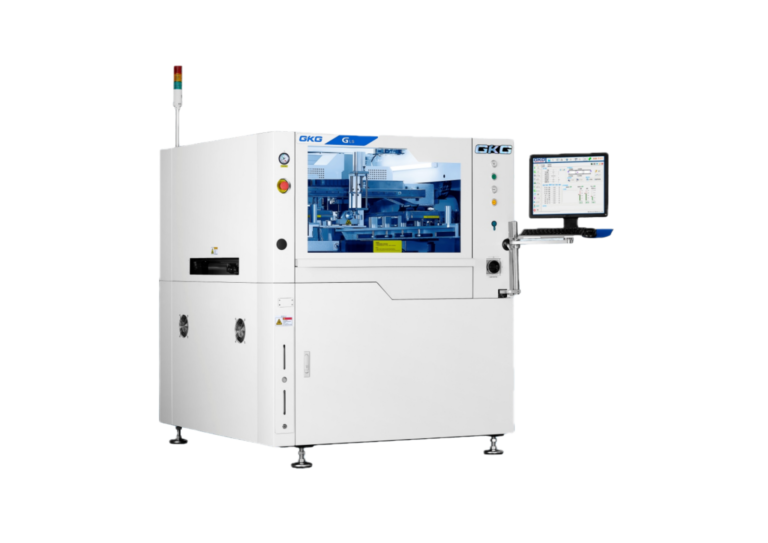
The SMT process begins with controlled solder paste printing.
Important factors include:
- Stencil design
- Solder paste
- PCB support
- Alignment
- Squeegee parameters
- Separation
- Stencil cleaning
Power-electronics PCBAs can include a mixture of pad sizes and component types, making the printing process an important foundation for downstream quality.
Step 2: SPI
SPI can inspect solder paste characteristics such as:
- Volume
- Height
- Area
- Position
This provides process information before component placement.
SPI can be particularly useful where the PCB contains:
- Fine-pitch components
- Dense layouts
- Small passives
- Different pad geometries
The required inspection strategy should follow the actual product and quality requirements.
Step 3: SMT Pick and Place
Renewable energy electronics can require placement of a broad range of components.
Machine selection should consider:
- Component range
- Placement accuracy
- Feeder capacity
- Tray handling
- PCB dimensions
- Component height
- Number of placements
- Target capacity
- Product mix
Do not select the machine based only on nominal CPH.
Placement Capacity Example
Suppose a control PCB contains:
500 SMT placements
and the target output is:
80 boards/hour
The theoretical placement demand is:
500 × 80 = 40,000 placements/hour
However, actual placement capacity should account for:
- Component mix
- Feeder arrangement
- Tray components
- Recognition
- PCB transfer
- Machine movement
- Production efficiency
The actual BOM should be used to configure the placement section.

Step 4: Reflow Soldering
After placement, the PCB enters the reflow oven.
The required thermal process depends on:
- Solder paste
- PCB construction
- Component requirements
- Copper distribution
- Thermal mass
Renewable energy power electronics can present additional thermal challenges due to thick copper, large copper areas, or larger components.
There is no universal reflow profile suitable for all renewable energy PCBAs.
Why Thermal Mass Matters
Consider two areas on the same PCB:
- Area A: Small passive components with limited copper.
- Area B: Large power components connected to significant copper areas.
These areas can heat at different rates.
The thermal profile should provide an acceptable process window for the complete assembly.
This is why actual PCB thermal profiling is important.
Step 5: AOI
After reflow, AOI can inspect visible characteristics such as:
- Missing components
- Component position
- Polarity
- Orientation
- Certain visible solder-joint conditions
- AOI can support defect detection and process monitoring.
However, hidden solder structures may require another inspection method.
X-Ray Inspection
X-ray may be useful for selected components such as:
- BGA
- Certain QFN applications
- Other hidden solder structures
Not every renewable energy PCB requires X-ray inspection.
The decision should be based on component design, product requirements, and inspection strategy.
Step 6: THT Component Preparation
Power electronics and energy-related PCBAs may contain THT components such as:
- Transformers
- Inductors
- Chokes
- Large electrolytic capacitors
- Relays
- Connectors
- Terminal blocks
- Fuses
- Selected power resistors
- Selected power semiconductor packages
Depending on the component, preparation can include:
- Lead cutting
- Forming
- Bending
- Straightening
- Sorting
- Kitting
This process should be included in line-capacity calculations.
Step 7: THT Insertion
THT insertion can be:
- Manual
- Semi-automatic
- Automatic
The correct approach depends on:
- Component geometry
- Lead structure
- Packaging
- Quantity per PCB
- Production volume
- Product mix
Large or irregular power components may still require manual insertion even in highly automated factories.
Manual Insertion Does Not Mean Uncontrolled Production
Manual THT stations can be organized with:
- Material kitting
- Visual work instructions
- Component identification
- Guided insertion
- Polarity control
- Pre-solder inspection
The objective is to create a controlled and balanced production process.
Step 8: Wave Soldering
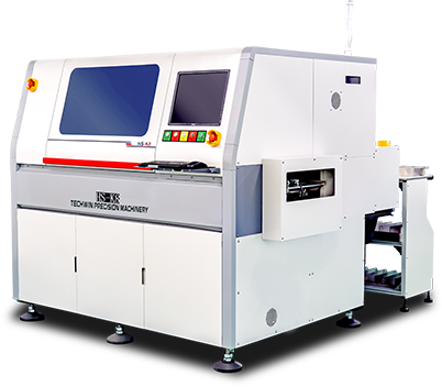
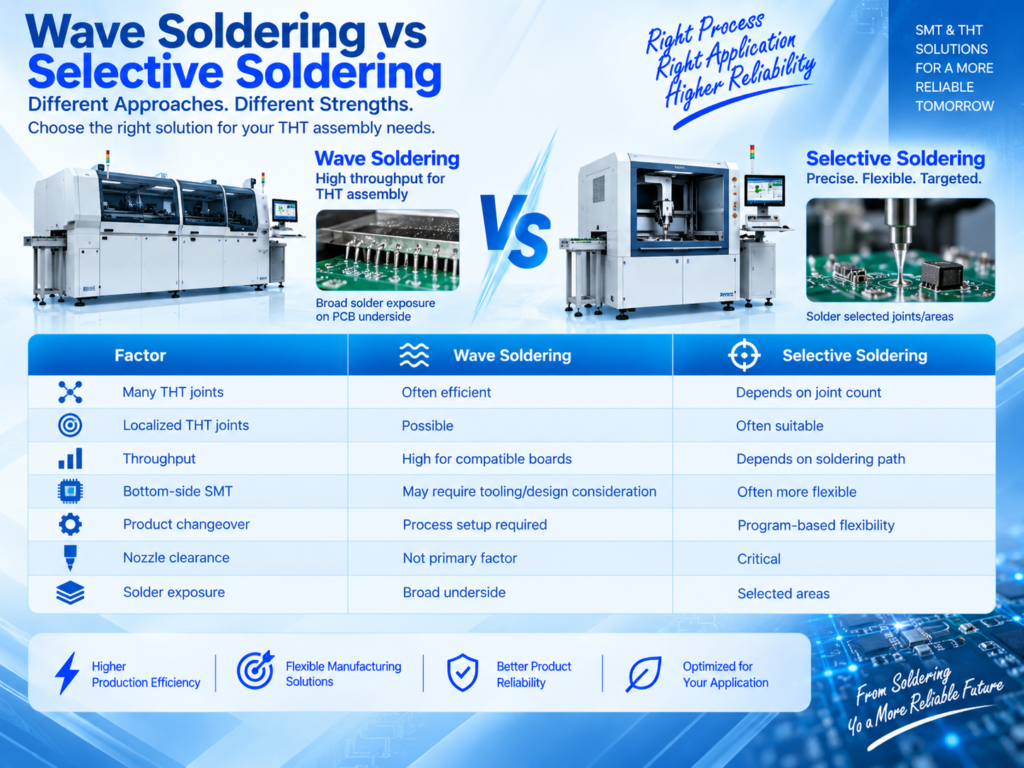
Wave soldering can be efficient when a PCB contains many compatible THT joints.
The process typically includes:
Fluxing → Preheating → Wave Soldering → Cooling
Important parameters include:
- Flux application
- Preheat
- Solder temperature
- Conveyor speed
- Wave stability
- PCB orientation
Power electronics PCBAs may require particular attention to thermal mass and hole fill.
Incomplete Hole Fill
Incomplete hole fill can be a concern when soldering high-thermal-mass THT joints.
Potential contributing factors include:
- PCB thermal mass
- Copper distribution
- Flux
- Preheat
- Solderability
- Lead/hole relationship
- Soldering conditions
Troubleshooting should evaluate the complete process rather than simply increasing solder temperature.
Step 9: Selective Soldering
Selective soldering can be considered when:
- THT joints are localized
- Bottom-side SMT components are present
- Wave exposure should be restricted
- Product mix is high
- Manual soldering requires automation
A typical process can include:
Fluxing → Preheating → Programmed Soldering → Cooling → Inspection
The machine configuration should be selected according to joint layout and required throughput.
Wave vs Selective Soldering for Renewable Energy PCBAs
Wave soldering may be attractive when:
- Many compatible THT joints are distributed across the PCB
- Higher continuous throughput is required
Selective soldering may be attractive when:
- THT joints are localized
- The underside contains sensitive SMT areas
- Programmable flexibility is important
Neither process is universally better.
PCB Support and Pallets
Large or heavy renewable energy PCBAs may require careful support during transport and soldering.
Depending on the process, manufacturers may use:
- Conveyor support
- Center support
- Fixtures
- Wave soldering pallets
Pallets can help protect or support selected PCB areas, but they also add:
- Tooling cost
- Thermal mass
- Cleaning
- Maintenance
- Storage
Their use should be based on the actual PCB.
Common Soldering Defects
Potential THT soldering defects include:
- Solder bridges
- Insufficient solder
- Incomplete hole fill
- Poor wetting
- Excessive solder
- Icicles
- Solder balls
Potential causes can involve:
PCB + Components + Flux + Preheat + Solder + Conveyor + Equipment
A systematic root-cause approach is more effective than changing one process parameter randomly.
Step 10: Electrical and Functional Testing
Testing requirements vary significantly across renewable energy products.
Depending on the PCBA, manufacturers may use:
- ICT
- Flying probe
- Programming
- Functional testing
- Communication testing
- Product-specific electrical testing
Certain power products may also require additional safety or high-voltage-related testing according to the actual product design and applicable requirements.
These tests should be defined by the product specification rather than assumed for every renewable energy PCB.
Conformal Coating for Renewable Energy Electronics
Some renewable energy PCBAs operate in environments where additional surface protection may be required.
Potential environmental factors can include:
- Humidity
- Condensation
- Dust
- Temperature variation
- Certain contaminants
- Corrosive environments
Depending on product design and enclosure, conformal coating may be considered.
A typical process is:
Testing → Cleaning/Surface Preparation → Selective Coating → Inspection → Flash-Off → Curing → Final Inspection
Not every renewable energy PCB requires conformal coating.
Coating Keep-Out Areas
Where selective coating is used, keep-out areas may include:
- Connectors
- Terminal contacts
- Test points
- Programming interfaces
- Switches
- Selected sensors
- Mechanical contact areas
The coating drawing should define these areas before programming the equipment.
Conformal Coating vs Potting
Conformal coating and potting are different protective strategies.
Conformal coating generally forms a relatively thin protective layer that follows the PCB surface.
Potting uses a larger volume of material to encapsulate part or all of an assembly.
The appropriate approach depends on:
- Environmental exposure
- Mechanical requirements
- Thermal design
- Repair requirements
- Product specification
Neither universally replaces the other.
High-Mix Renewable Energy PCBA Manufacturing
Renewable energy manufacturers may produce several board types for:
- Control
- Communication
- Power conversion
- Monitoring
- Battery management
A flexible line may prioritize:
- Feeder capacity
- Fast changeover
- Recipe management
- Flexible placement
- Manual/semi-automatic THT insertion
- Selective soldering
- Flexible testing
This can be more practical than maximizing machine speed.
Medium-Volume Production Line
A medium-volume configuration may use:
Automatic Loader → Automatic Printer → SPI → Pick and Place Machine(s) → Reflow → AOI → THT Preparation → Balanced Insertion → Wave/Selective Soldering → Inspection → Testing
Optional coating can be added downstream where required.
Higher-Volume Production
For stable higher-volume products, manufacturers can consider:
Automatic Loading → Printing → SPI → Multiple Placement Machines → Reflow → AOI → Automated/Semi-Automated THT Assembly → Soldering → Inspection → Parallel Testing → Automatic Unloading
Traceability can be integrated where required.
Line Balancing
Evaluate the entire process:
Printing → SPI → Placement → Reflow → AOI → THT → Soldering → Inspection → Testing
The bottleneck determines finished output.
Useful metrics include:
- Cycle time
- Takt time
- First-pass yield
- Downtime
- Rework
- Changeover
- WIP
- Equipment utilization
Do not optimize placement capacity while ignoring testing or THT assembly.
Material Management
Renewable energy PCBAs may contain large and diverse components.
Plan material handling for:
- SMT reels
- Trays
- THT components
- Large components
Moisture-sensitive materials where applicable
Feeders
Work-in-process PCBAs
Material preparation should support the required takt time.
Factory Layout
A complete factory layout can include:
- Incoming material
- Material storage
- SMT production
- THT preparation
- THT insertion
- Soldering
- Inspection
- Testing
- Rework
- Coating where required
- Finished PCBA storage
Large PCBAs and components may require additional handling space.
Utilities
Depending on equipment configuration, utilities may include:
- Electrical power
- Compressed air
- Exhaust
- HVAC/environmental control
- Nitrogen where required
- Network connections
Soldering and coating processes can have additional exhaust requirements.
Plan utilities before equipment installation.
New vs Pre-Owned Equipment
Renewable energy manufacturers can consider both new and suitable pre-owned SMT equipment.
New equipment may be attractive where manufacturers prioritize:
- Current technology
- High utilization
- Advanced automation
- Factory integration
Pre-owned equipment can be attractive where:
- Lower initial investment is important
- Equipment condition is verified
- Required production capability is available
- Spare parts and support remain accessible
A hybrid new + pre-owned line can also provide a practical investment strategy.
Total Cost of Ownership
Do not evaluate a production line by equipment price alone.
A simplified model is:
PCBA Line TCO = Equipment + Feeders + Tooling + Installation + Utilities + Training + Spare Parts + Maintenance + Energy + Labor + Downtime + Process Losses
A lower machine purchase price does not automatically produce a lower manufacturing cost.
Renewable Energy PCBA Solutions from Fuliu Electronics
Established in 2014, Fuliu Electronics is dedicated to providing customers with high-quality PCBA intelligent manufacturing solutions and services.
With extensive experience in the SMT industry, we specialize in dependable equipment, professional technical support, and complete SMT and PCBA production line solutions.
Our equipment portfolio includes SMT pick and place machines from Fuji, Panasonic, ASM, Yamaha, JUKI, and Hanwha, together with ERSA reflow ovens from Germany, MagicRay SPI/AOI inspection systems, automatic solder paste printers, supporting PCBA equipment, pre-owned SMT equipment, SMT spare parts, machine leasing, and maintenance services.
Frequently Asked Questions
PCBAs can be used in solar inverters, energy storage systems, battery management electronics, wind power controls, energy monitoring systems, power conversion equipment, and EV charging infrastructure.
Many products do, depending on design. SMT can support dense control electronics, while THT may be used for selected transformers, inductors, relays, connectors, terminals, capacitors, and other power components.
Thick copper, large copper areas, and large components can change how the PCB heats during reflow and THT soldering, affecting the process window.
It depends on THT joint distribution, PCB underside design, production volume, and product mix. Wave soldering can suit many compatible joints, while selective soldering can suit localized THT areas.
No. Coating depends on environmental exposure, enclosure design, PCB requirements, coating compatibility, and product specifications.
Not universally. X-ray can be useful for selected hidden solder structures where optical inspection is insufficient.