Printed Circuit Board Assembly (PCBA) is the foundation of modern electronics manufacturing. From smartphones and automotive control systems to industrial automation equipment and medical devices, almost every electronic product relies on a reliable PCB assembly process.
For manufacturers, investors, procurement managers, and engineers, understanding the PCB assembly process step by step is essential for improving product quality, reducing production costs, and achieving stable manufacturing performance.
As electronic products become increasingly compact and complex, modern factories have adopted highly automated SMT production lines and DIP assembly systems to improve efficiency and consistency. Whether you are planning to build a new PCB assembly factory or upgrade an existing production line, understanding each production stage helps ensure better investment decisions and manufacturing outcomes.
In this guide, we will walk through the complete PCB assembly process, explain the equipment involved, discuss quality control measures, and provide practical insights for building an efficient PCB assembly line.
What is PCB Assembly?
Before discussing the manufacturing process, it is important to understand the difference between PCB and PCBA.
PCB (Printed Circuit Board)
A PCB is a bare board that contains conductive traces used to connect electronic components.
PCBA (Printed Circuit Board Assembly)
A PCBA is a completed circuit board after electronic components have been mounted and soldered onto the PCB.
The PCB assembly process transforms a blank circuit board into a functional electronic module ready for installation in electronic products.
Modern PCB assembly generally involves two technologies:
Surface Mount Technology (SMT)
Components are mounted directly onto the PCB surface.
Through-Hole Technology (DIP/THT)
Component leads are inserted through holes and soldered on the opposite side of the PCB.
Most modern electronic products use a combination of SMT and DIP assembly processes.
PCB Assembly Process Overview
The typical PCB assembly process consists of the following steps:
- Incoming Material Inspection
- Solder Paste Printing
- SPI Inspection
- SMT Component Placement
- Reflow Soldering
- AOI Inspection
- DIP Component Insertion
- Wave Soldering
- Functional Testing
- Final Inspection and Packaging
Step 1: Incoming Material Inspection
Quality control begins before production starts.
Incoming materials typically include:
- Printed circuit boards
- Electronic components
- ICs and connectors
- Solder paste
- Packaging materials
Manufacturers inspect:
PCB Quality
Checking for scratches, warpage, contamination, and dimensional accuracy.
Component Verification
Ensuring part numbers and specifications match production requirements.
Moisture-Sensitive Components
Components such as BGA packages require strict moisture control to prevent damage during soldering.
Material Traceability
Barcode systems help track materials throughout the production process.
Proper incoming inspection significantly reduces manufacturing defects later in production.
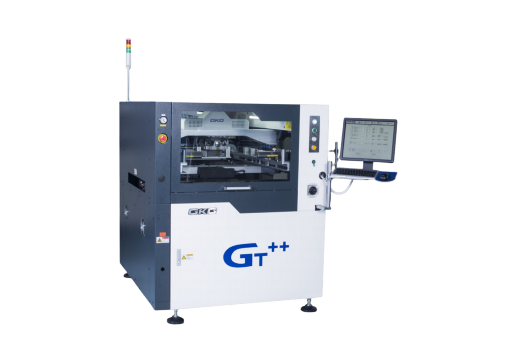
Step 2: Solder Paste Printing
Solder paste printing is the first SMT process.
A solder paste printer applies solder paste onto designated PCB pads using a precision stencil.
Key Factors Affecting Printing Quality
- Stencil design
- Solder paste quality
- Printing pressure
- Alignment accuracy
- Environmental conditions
Common Printing Defects
- Insufficient solder
- Excessive solder
- Offset printing
- Smearing
Because approximately 60–70% of SMT defects originate during solder paste printing, this step is critical for production success.
Step 3: SPI Inspection
SPI stands for Solder Paste Inspection.
SPI systems inspect solder paste deposits immediately after printing.
What SPI Measures
- Solder paste volume
- Height
- Area
- Position
Defects Detected
- Insufficient solder
- Excessive solder
- Misalignment
- Potential bridging risks
By identifying printing defects early, SPI significantly improves first-pass yield and reduces rework costs.
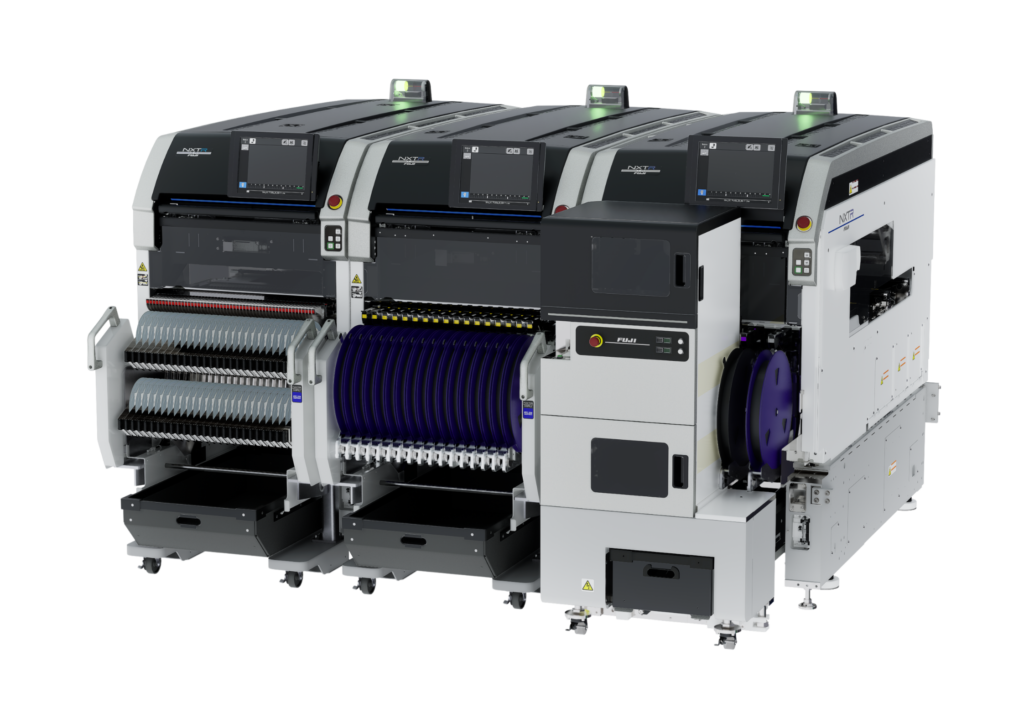
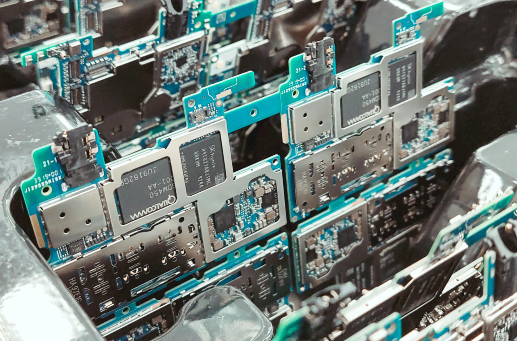
Step 4: SMT Component Placement
After solder paste inspection, components are mounted onto the PCB using high-speed pick and place machines.
Main Components of Placement Equipment
- Feeders
- Placement heads
- Vision alignment systems
- Conveyor systems
Components Commonly Mounted
- Resistors
- Capacitors
- ICs
- BGAs
- LEDs
- Connectors
Modern SMT machines can place tens of thousands of components per hour while maintaining micron-level accuracy.
Placement accuracy directly impacts soldering quality and final product reliability.
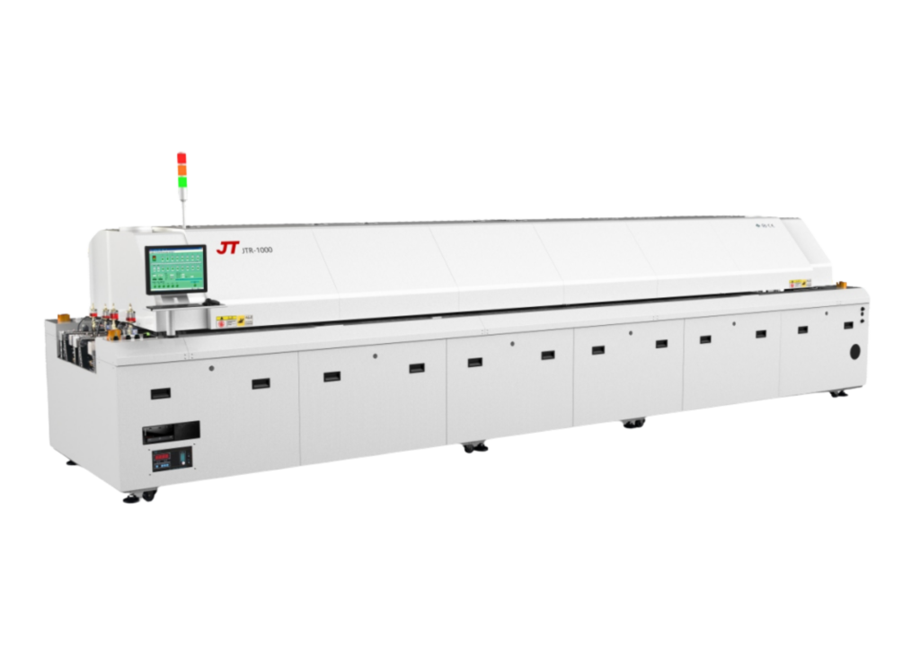
Step 5: Reflow Soldering
Once components are placed, the PCB enters the reflow oven.
The oven heats the PCB according to a controlled temperature profile, melting solder paste and creating permanent electrical connections.
Typical Reflow Zones
Preheating Zone
Gradually increases PCB temperature.
Soaking Zone
Activates flux and stabilizes temperature.
Reflow Zone
Melts solder paste.
Cooling Zone
Solidifies solder joints.
Common Reflow Defects
- Tombstoning
- Solder bridging
- Cold solder joints
- Voiding
Proper temperature profile optimization is essential for high-quality solder joints.
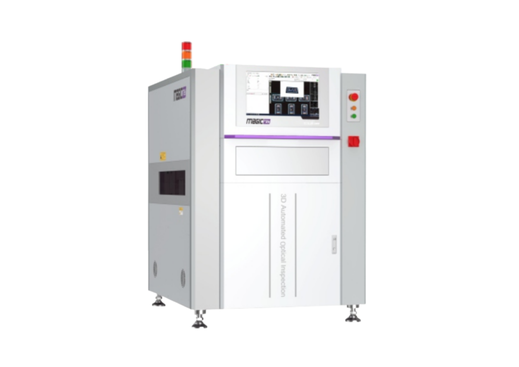
Step 6: AOI Inspection
AOI (Automatic Optical Inspection) is one of the most important quality control steps.
AOI systems use high-resolution cameras and image processing software to inspect assembled PCBs.
AOI Detects
- Missing components
- Wrong components
- Polarity errors
- Misalignment
- Solder bridges
- Insufficient solder
Step 7: DIP Component Insertion
Some components cannot be mounted using SMT technology.
Examples include:
- Transformers
- Large capacitors
- Power connectors
- Relays
These components are assembled using Through-Hole Technology (THT).
Insertion Methods
Manual Insertion
Suitable for low-volume production.
Automatic Insertion
Suitable for high-volume manufacturing.
DIP assembly provides strong mechanical connections and enhanced durability.
Step 8: Wave Soldering
After component insertion, boards enter the wave soldering process.
Wave Soldering Stages
Fluxing
Flux removes oxidation.
Preheating
Prepares PCB for soldering.
Solder Wave
PCB passes over molten solder.
Cooling
Solidifies solder joints.
Advantages of Wave Soldering
- High efficiency
- Consistent soldering quality
- Suitable for mass production
Common Defects
- Bridging
- Icicles
- Insufficient solder
Process optimization helps minimize these issues.
Step 9: Functional Testing
Even visually perfect PCBs may contain electrical defects.
Functional testing verifies product performance.
Common Testing Methods
ICT (In-Circuit Testing)
Checks electrical connections and component values.
FCT (Functional Circuit Testing)
Simulates actual operating conditions.
Burn-In Testing
Operates products continuously under controlled conditions.
Testing ensures only qualified products proceed to shipment.
Step 10: Final Inspection and Packaging
Before shipment, products undergo final quality verification.
Inspection Includes
- Visual inspection
- Label verification
- Traceability confirmation
- Packaging inspection
Packaging Requirements
- ESD protection
- Moisture barrier packaging
- Shock-resistant transportation packaging
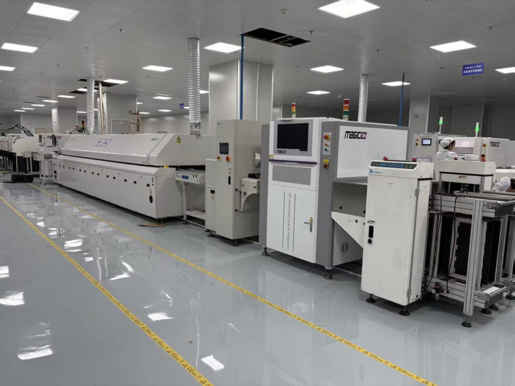
SMT Equipment Used in PCB Assembly
SMT Line Equipment
- PCB Loader
- Solder Paste Printer
- SPI System
- Pick and Place Machine
- Reflow Oven
- AOI System
- PCB Unloader
DIP Line Equipment
- Conveyor System
- Manual Insertion Stations
- Wave Soldering Machine
- Inspection Stations
Choosing the right equipment directly affects production efficiency, product quality, and return on investment.
How to Build an Efficient PCB Assembly Line
When planning a PCB assembly factory, consider:
Factory Layout Planning
Optimize material flow and production efficiency.
Capacity Planning
Calculate production requirements before selecting equipment.
Automation Level
Balance investment cost with labor savings.
Inspection Systems
Integrate SPI, AOI, and testing systems.
Future Expansion
Reserve space for production growth.
A well-designed SMT production line can significantly improve manufacturing profitability.
Real-World PCB Assembly Applications
Consumer Electronics
- Smartphones
- Tablets
- Smart home products
Automotive Electronics
- ECU modules
- Vehicle sensors
- Safety systems
LED Manufacturing
- LED drivers
- Lighting control modules
Industrial Electronics
- PLC controllers
- Power management boards
Each industry has unique PCB assembly requirements and quality standards.

Why Turnkey PCB Assembly Solutions Are Growing
Many manufacturers now prefer turnkey SMT solutions because they offer:
- Faster factory deployment
- Reduced project risk
- Integrated equipment compatibility
- Simplified supplier management
- Better technical support
Turnkey solutions help investors reduce uncertainty while accelerating production startup.
About FULIU Electronics
FULIU Electronics specializes in turnkey SMT and PCB assembly production line solutions for global manufacturers.
Our services include:
- SMT production line equipment
- PCB assembly equipment supply
- SPI and AOI inspection systems
- Reflow soldering equipment
- Wave soldering machines
- Factory layout planning
- Installation and operator training
- Global delivery and after-sales support
With extensive experience in SMT factory setup and PCBA manufacturing solutions, we help customers build reliable, efficient, and cost-effective PCB assembly facilities worldwide.
Conclusion
The PCB assembly process is a carefully controlled sequence of manufacturing steps that transforms bare circuit boards into fully functional electronic products.
From incoming material inspection and solder paste printing to AOI inspection, wave soldering, and final testing, every stage plays a critical role in product quality and manufacturing efficiency.
Successful PCB assembly depends on:
- High-quality equipment
- Stable production processes
- Advanced inspection systems
- Professional technical support
Whether you are building a new SMT production line or upgrading an existing PCBA factory, working with an experienced turnkey SMT solution provider can help maximize efficiency, quality, and long-term profitability.
Contact FULIU Electronics today to discuss your PCB assembly production line requirements and discover the best solution for your manufacturing goals.