
In modern SMT (Surface Mount Technology) manufacturing, achieving reliable solder joints starts long before components are placed on a printed circuit board. One of the most critical steps is ensuring that solder paste is printed accurately and consistently. Even minor printing defects can lead to assembly failures, costly rework, and reduced production yield.
This is where SPI inspection (Solder Paste Inspection) plays a vital role. By automatically measuring solder paste deposits immediately after the printing process, SPI helps manufacturers detect defects before they become expensive production problems.
In this guide, we’ll explain what SPI inspection is, how it works, why it’s essential for PCB assembly, and how it differs from other inspection technologies such as AOI.
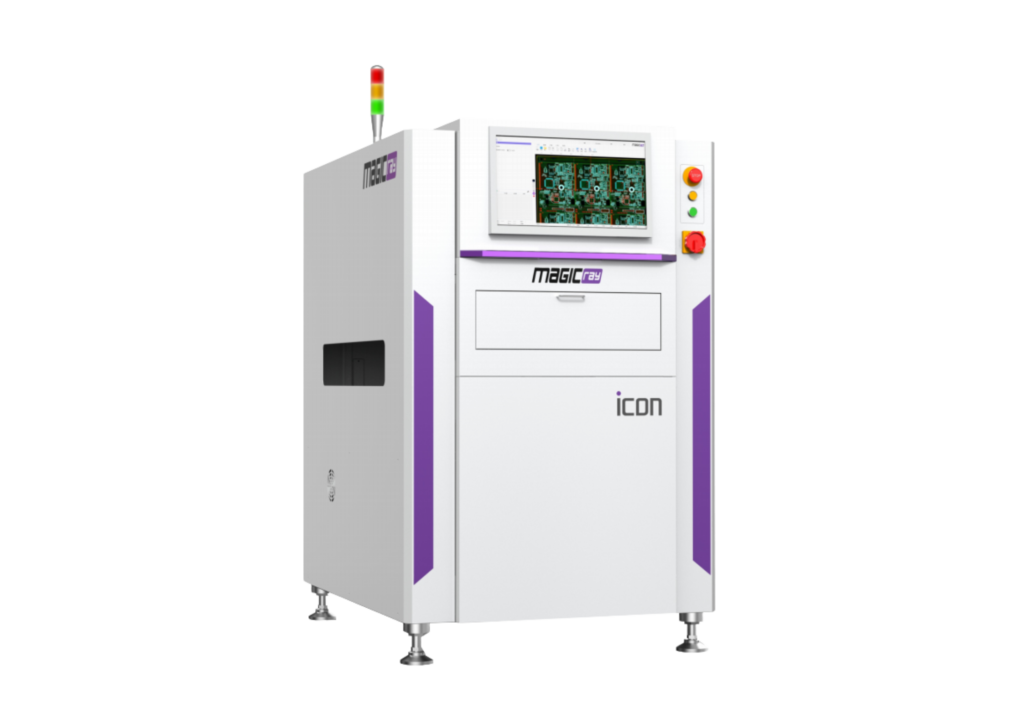
What Is SPI Inspection?
SPI (Solder Paste Inspection) is an automated inspection process used in SMT production to measure the quality of solder paste printed onto a PCB before electronic components are placed.
Unlike visual inspection, SPI systems use high-resolution cameras, laser scanning, or 3D optical measurement technology to evaluate whether the solder paste has been deposited correctly.
SPI is typically installed immediately after the automatic solder paste printer and before the pick and place machine, making it the first automated quality checkpoint in the SMT production line.
Why Is SPI Inspection Important?
Industry studies show that a large percentage of SMT assembly defects originate during the solder paste printing process. If these defects are not identified early, they can lead to component placement issues, poor solder joints, or complete product failure.
SPI inspection helps manufacturers:
- Detect printing defects before assembly
- Reduce rework and scrap
- Improve first-pass yield (FPY)
- Increase production efficiency
- Maintain consistent solder quality
- Lower manufacturing costs
By preventing defective boards from moving downstream, SPI saves both time and resources.
How Does SPI Inspection Work?
A typical SPI inspection process consists of several stages.
Step 1: Solder Paste Printing
An automatic solder paste printer applies solder paste to PCB pads through a precision stencil.
The quality of this step directly affects the entire assembly process.
Step 2: 3D Measurement
The SPI machine scans every solder paste deposit using advanced optical technology.
Rather than checking only the surface, modern SPI systems measure three-dimensional characteristics, including:
- Paste volume
- Paste height
- Paste area
- Paste position
- Paste shape
These measurements provide far greater accuracy than traditional 2D inspection.
Step 3: Data Analysis
Inspection software compares the measured solder paste deposits with predefined tolerance limits or CAD data.
If any deposit falls outside the acceptable range, the board is automatically flagged for review.
Step 4: Feedback and Process Improvement
Many advanced SPI systems communicate directly with solder paste printers.
When trends indicate printing deviations, the printer can be adjusted before additional defective boards are produced.
This closed-loop process helps maintain stable production quality.
What Defects Can SPI Detect?
SPI systems identify a wide range of solder paste printing defects.
Common defects include:
- Insufficient solder paste
- Excess solder paste
- Missing solder paste
- Offset printing
- Bridging between pads
- Poor stencil release
- Smearing
- Uneven paste height
- Incorrect paste volume
- Incomplete aperture filling
Detecting these issues before component placement significantly improves manufacturing yield.
Benefits of SPI Inspection
Improve First-Pass Yield
Correcting solder paste defects early reduces downstream failures and increases the percentage of boards that pass inspection on the first attempt.
Reduce Rework Costs
Repairing printing defects before components are mounted is much easier and less expensive than reworking fully assembled PCBs.
Increase Production Efficiency
Automatic inspection eliminates the need for time-consuming manual checks while enabling continuous high-speed production.
Improve Process Stability
Real-time monitoring helps manufacturers maintain consistent printing quality throughout long production runs.
Support Data-Driven Manufacturing
Modern SPI systems generate valuable production data that can be used to optimize printing parameters and improve long-term process control.
Where Is SPI Installed in an SMT Production Line?
A standard SMT workflow typically follows this sequence:
- PCB Loader
- Automatic Solder Paste Printer
- SPI Inspection
- Pick and Place Machine
- Reflow Oven
- AOI Inspection
- Functional Testing
- PCB Unloader
Positioning SPI immediately after printing allows manufacturers to correct problems before components are placed, preventing unnecessary material waste.
How to Choose an SPI Inspection System
Selecting the right SPI machine depends on several production requirements.
Measurement Accuracy
High-resolution 3D measurement provides more reliable defect detection, especially for fine-pitch components.
Inspection Speed
The inspection system should match the throughput of the SMT production line to avoid creating bottlenecks.
Closed-Loop Capability
Advanced SPI systems can automatically communicate with solder paste printers to optimize printing performance.
Software Functions
Look for features such as:
- Statistical Process Control (SPC)
- Trend analysis
- Production reporting
- CAD import
- Automatic programming
- MES integration
These capabilities support smart manufacturing initiatives.
Best Practices for SPI Inspection
Manufacturers can maximize SPI performance by following several best practices.
Regularly calibrate the SPI machine.
Maintain clean stencils and printer equipment.
Use high-quality solder paste.
Monitor environmental conditions.
Analyze production trends using SPC data.
Integrate SPI with AOI for complete process control.
Train operators to interpret inspection results accurately.
Consistent process management leads to higher production quality and fewer defects.
Why Choose Fuliu Electronics?
Established in 2014, Fuliu Electronics is dedicated to providing customers with high-quality PCBA intelligent manufacturing solutions and comprehensive technical services.
With extensive experience in the SMT industry, Fuliu Electronics supplies complete SMT production line solutions featuring internationally recognized brands such as Fuji, Panasonic, ASM, Yamaha, JUKI, and Hanwha, together with MagicRay SPI/AOI inspection systems, ERSA reflow ovens, automatic solder paste printers, refurbished SMT equipment, SMT spare parts, equipment leasing, and maintenance services.
Serving customers across India, Vietnam, the Philippines, Indonesia, the Middle East, South Africa, and Europe, Fuliu Electronics helps manufacturers build intelligent SMT production lines with advanced inspection technologies that improve product quality, process stability, and manufacturing efficiency.
Conclusion
SPI inspection is one of the most important quality control processes in modern SMT manufacturing. By accurately measuring solder paste deposits before component placement, SPI enables manufacturers to detect printing defects at the earliest possible stage, reducing rework, improving first-pass yield, and lowering production costs.
When combined with AOI inspection, high-quality printing equipment, and a well-optimized SMT production line, SPI becomes a powerful tool for achieving consistent, reliable PCB assembly quality. As electronics continue to become smaller and more complex, investing in advanced SPI technology is an increasingly valuable strategy for manufacturers seeking higher productivity and long-term competitiveness.
Frequently Asked Questions
SPI (Solder Paste Inspection) is an automated process that measures solder paste deposits on a PCB after printing and before component placement to ensure printing quality.
SPI identifies solder paste defects early, preventing assembly problems, reducing rework, improving first-pass yield, and increasing production efficiency.
SPI can detect insufficient or excessive solder paste, missing paste, offset printing, bridging, uneven paste height, incorrect paste volume, and other printing defects.
SPI inspects solder paste immediately after printing, while AOI inspects component placement and solder joints after assembly or reflow soldering.
Although smaller operations may rely on manual inspection, SPI is highly recommended for medium- and high-volume SMT manufacturing where consistent quality and process control are essential.
Yes. By detecting printing defects before component placement, SPI reduces scrap, minimizes rework, and helps maintain stable, efficient production.