
Smart home products combine electronics, connectivity, sensors, control functions, and user interfaces into increasingly compact devices.
Common applications include:
- Smart switches
- Smart plugs
- Smart lighting controllers
- Smart thermostats
- Smart door locks
- Smart sensors
- Smart hubs
- Security devices
- Smart cameras
- Home energy-management devices
- Smart appliances
- Wireless control modules
Inside these products, a relatively small PCB may combine:
- Microcontrollers
- Memory devices
- Wireless communication modules
- Sensors
- LEDs
- Buttons
- Connectors
- Power-management components
- Relays
- Antenna-related structures
- Small passive components
This combination creates specific requirements for PCB assembly for smart home devices.
A suitable manufacturing process may include:
PCB Loading → Solder Paste Printing → SPI → SMT Placement → Reflow → AOI → Programming → Functional Testing → PCB Unloading
Depending on the product, THT assembly, X-ray inspection, cleaning, conformal coating, barcode identification, and additional testing may also be required.
The correct production line should be based on the actual PCB, BOM, product architecture, target volume, product mix, and quality requirements.
What Types of Smart Home Devices Use PCB Assemblies?
Smart home electronics cover a broad range of products.
Smart Lighting
PCBs may control:
- LED lighting
- Dimming
- Wireless communication
- Power management
- User interfaces
Smart Sensors
Examples include:
- Temperature sensors
- Humidity sensors
- Motion sensors
- Door/window sensors
- Light sensors
- Environmental sensors
These products may prioritize compact design and sensor performance.
Smart Plugs and Switches
These can combine:
- MCU
- Wireless communication
- Power electronics
- Relays
- Buttons
- LEDs
- Protection components
Power-handling requirements can make the PCB assembly process different from a low-power sensor board.
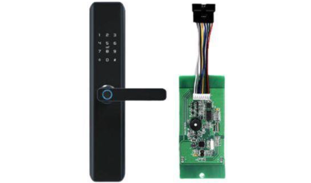
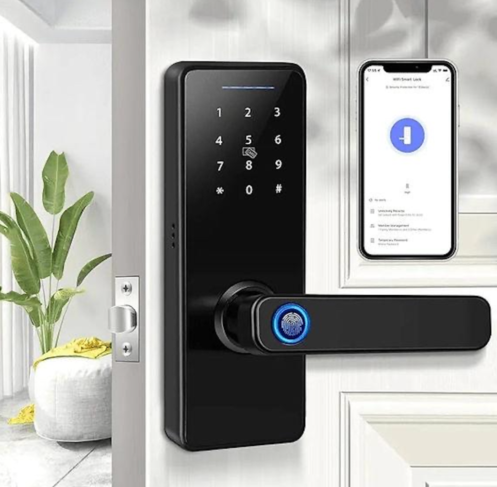
Smart Locks and Security Devices
These may contain:
- Wireless modules
- Motor-control electronics
- Sensors
- Battery-management circuits
- User interfaces
Smart Hubs and Gateways
These can contain more complex processing and communication electronics, potentially including multiple wireless technologies.
The manufacturing process therefore depends strongly on the product architecture.
Why Smart Home PCB Assembly Can Be Challenging
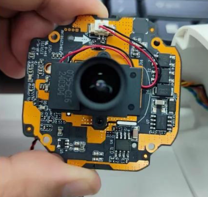
Smart home PCBs can combine several technologies in a small physical area.
A board may contain:
- 0201/0402 passive components
- Fine-pitch ICs
- QFN packages
- BGA packages
- Wireless modules
- Sensors
- Connectors
- LEDs
- Relays
- Power components
Manufacturers must therefore manage:
- Miniature component placement
- Solder paste printing
- Reflow
- RF-related components
- Component orientation
- Inspection
- Programming
- Functional testing
- Product changeover
The challenge is not simply achieving high placement speed.
The complete production process must remain stable.
Start with PCB and BOM Analysis
Before selecting SMT equipment, collect the actual product data.
Important information includes:
- PCB dimensions
- PCB thickness
- Panel dimensions
- PCB weight
- BOM
- Component packages
- Number of placements
- Smallest component
- Largest component
- Maximum component height
- Wireless modules
- Sensors
- Connectors
- THT components
- Target production volume
- Product mix
For wireless products, also identify any components or areas that require special handling during assembly and testing.
Typical Smart Home PCBA Production Flow
A typical SMT process is:
PCB Loader → Automatic Solder Paste Printer → SPI → Pick and Place Machine → Reflow Oven → AOI → Programming → Functional Testing → PCB Unloader
For products with THT components:
SMT Assembly → Reflow → AOI → THT Insertion → Wave/Selective Soldering → Inspection → Programming → Functional Testing
Optional processes may include:
X-Ray → Cleaning → Conformal Coating → Curing → Final Inspection
Not every smart home device requires all of these processes.
Step 1: PCB Loading
Automatic PCB loading can improve material flow for medium- and high-volume production.
The loader should support the actual:
- PCB size
- Thickness
- Weight
- Panel format
- Conveyor requirements
For small smart home devices, panelization may also influence production efficiency.
Panelization for Smart Home PCBs
Small PCBs can sometimes be manufactured as panels containing multiple individual boards.
Panelization can improve:
- Material handling
- SMT throughput
- Production efficiency
However, panel design should also consider:
- Depanelization
- Board stress
- Component placement
- Edge clearance
- Warpage
The correct panel configuration should be determined during PCB design and manufacturing planning.
Step 2: Solder Paste Printing
Solder paste printing establishes the foundation for SMT solder joints.
Important factors include:
- Stencil design
- Paste selection
- PCB support
- Alignment
- Squeegee pressure
- Printing speed
- Separation
- Stencil cleaning
Smart home PCBs often contain dense layouts and small components, making controlled solder paste deposition particularly important.
Potential defects include:
- Insufficient paste
- Excess paste
- Offset
- Bridging
- Inconsistent deposits
Step 3: SPI Inspection
SPI can inspect solder paste before component placement.
Depending on the system, measurements can include:
- Height
- Volume
- Area
- Position
SPI provides an opportunity to identify printing problems before components are placed.
For high-density smart home PCBs, this can help improve process visibility.
Step 4: SMT Placement
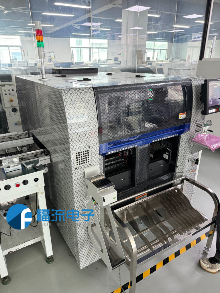
Pick and place equipment should be selected according to the actual component range.
Important factors include:
- Smallest component
- Largest component
- Placement accuracy
- Component height
- Feeder capacity
- Tray support
- Component recognition
- PCB dimensions
- Placement quantity
- Product mix
This is particularly important for smart home products because a single PCB can contain miniature passives alongside wireless modules, connectors, sensors, and other larger components.
Placement Capacity Example
Suppose a smart home controller contains: 300 SMT placements
and the target production rate is: 150 boards/hour
The theoretical placement requirement is: 300 × 150 = 45,000 placements/hour
However, actual requirements should account for:
- Component mix
- Feeder arrangement
- Recognition
- Tray components
- PCB transfer
- Changeover
- Machine efficiency
Therefore, rated CPH should not be treated as actual finished-board capacity.
Step 5: Wireless Module Placement
Many smart home products use communication modules for technologies such as:
- Wi-Fi
- Bluetooth
- Zigbee
- Thread
- Other wireless protocols
The exact technology depends on the product.
Modules may contain fine-pitch or specialized components and can require careful handling during placement and soldering.
Manufacturers should evaluate:
- Component orientation
- Placement accuracy
- Package structure
- Solder-pad design
- Reflow compatibility
- Inspection requirements
- RF Considerations
PCB assembly equipment does not determine wireless performance by itself.
RF performance can also depend on:
- PCB layout
- Antenna design
- Grounding
- Component placement
- Mechanical enclosure
- Material selection
Therefore, the manufacturing process should follow the PCB designer’s requirements.
Step 6: Reflow Soldering
After placement, the PCB passes through the reflow oven.
The thermal profile depends on:
- Solder paste
- PCB construction
- Component requirements
- Copper distribution
- Thermal mass
Wireless modules and miniature components should be evaluated according to their applicable process specifications.
There is no universal reflow profile for all smart home PCBs.
Actual thermal profiling should use the real PCB and materials.
Step 7: AOI Inspection
AOI can inspect visible characteristics including:
- Missing components
- Position
- Orientation
- Polarity
- Certain visible solder conditions
- AOI can help identify assembly defects after reflow.
However, it cannot directly inspect every hidden solder connection.
When Is X-Ray Required?
X-ray may be considered for selected applications involving:
- BGA
- QFN
- Hidden solder joints
- Other packages with limited optical access
- Not every smart home PCBA requires X-ray.
The inspection method should be selected according to the actual package structure and product requirements.
Step 8: THT Assembly
Some smart home products can contain THT components such as:
- Relays
- Connectors
- Terminal blocks
- Switches
- Large capacitors
- Selected power components
These components can be inserted:
- Manually
- Semi-automatically
- Automatically
The appropriate method depends on component geometry, packaging, volume, and product mix.
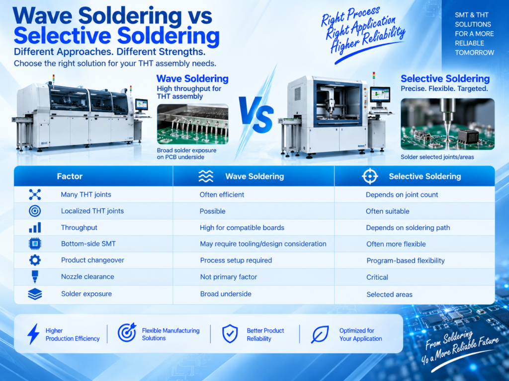
Wave vs Selective Soldering
If a smart home PCB contains many compatible THT joints, wave soldering may be considered.
Selective soldering may be more suitable when:
- THT joints are localized
- Bottom-side SMT components are present
- Wave exposure should be restricted
- Product mix is high
- Neither process is universally better.
Step 9: Programming
Smart home devices frequently require software or firmware programming.
Depending on the product, programming may occur:
- Before functional testing
- During functional testing
- After assembly
The programming process may involve:
- Firmware
- Device configuration
- Serial number assignment
- Product identification
- Communication parameters
The exact process should follow the product architecture.
Step 10: Functional Testing
For smart home devices, functional testing can be especially important.
Depending on the product, testing may include:
- Power-on testing
- Communication testing
- Button testing
- LED testing
- Sensor testing
- Relay testing
- Wireless communication
- I/O testing
- Current consumption
- Product-specific functional verification
For connected products, the test system may need to communicate with the device during testing.
Testing Can Become the Bottleneck
Consider:
The finished production capacity is approximately: 60 boards/hour
Even if the SMT section can produce 150+ boards/hour, final output remains limited by testing.
Parallel Testing
Suppose:
- Functional test time = 90 seconds
- Required takt = 30 seconds
A simplified calculation gives: 90 ÷ 30 = 3 parallel test positions
Actual capacity should also include:
- Loading
- Unloading
- Test fixture handling
- Retest
- Operator time
Testing should therefore be designed together with the SMT line.
Smart Home Product Traceability
Traceability requirements vary by product and customer.
Potential records include:
- PCB serial number
- Product model
- PCB revision
- Production time
- Machine
- Program
- Component information
- Material lot
- Solder paste lot
- SPI results
- Reflow data
- AOI results
- Programming records
- Functional test results
Barcode or QR-code identification can connect manufacturing data to individual products.
Recipe Management
A smart home manufacturer may produce several versions of a product.
Recipes may exist for:
- Printer
- SPI
- Pick and place
- Reflow
- AOI
- Programming
- Testing
Correct product identification can help prevent the wrong production program from being loaded.
This becomes particularly useful for factories producing multiple models.
High-Mix Smart Home Electronics
Smart home manufacturers may produce many models, such as:
- Smart plugs
- Sensors
- Controllers
- Hubs
- Switches
- Security devices
These products can have different BOMs and PCB dimensions.
For high-mix production, consider:
- Feeder capacity
- Offline setup
- Fast changeover
- Flexible placement
- Recipe management
- Barcode verification
- Material kitting
Maximum CPH may not be the most important performance indicator.
Changeover Management
A changeover can involve:
- Stopping the line
- Removing feeders
- Preparing new components
- Loading the new program
- Verifying materials
- Running first boards
- Confirming quality
Offline feeder preparation can reduce production downtime.
Material Management
Smart home PCBs can contain many different component types.
Material control should consider:
- SMT reels
- Trays
- Moisture-sensitive devices where applicable
- Wireless modules
- Sensors
- Connectors
- THT components
Line-side material should be prepared according to actual production requirements.
Common Smart Home SMT Defects
Potential defects include:
- Missing components
- Misalignment
- Solder bridges
- Insufficient solder
- Tombstoning
- Polarity errors
- Component damage
- Incorrect component placement
Root-cause analysis should consider:
PCB Design + Solder Paste + Printing + Placement + Reflow + Component Quality
rather than focusing on one machine alone.
Conformal Coating for Smart Home PCBs
Some smart home products may operate in environments where additional PCB protection is useful.
Examples can include devices exposed to:
- Humidity
- Condensation
- Dust
- Temperature changes
- Certain contaminants
Potential applications may include selected:
- Sensors
- Outdoor-connected devices
- Control boards
- Environmental monitoring electronics
- However, not every smart home PCB requires conformal coating.
Coating Keep-Out Areas
If coating is used, keep-outs may include:
- Connectors
- Buttons
- Test points
- Programming interfaces
- Contacts
- Selected sensors
- Mechanical interfaces
Selective coating can control application around these areas.
The coating material, valve, curing process, and PCB geometry should be evaluated together.
Cleaning Before Coating
Cleaning requirements depend on:
- Flux chemistry
- PCB cleanliness requirements
- Coating material
- Process validation
- Product requirements
A suitable no-clean process may not require the same cleaning process as a conventional flux system.
There is no universal rule that every smart home PCBA must be cleaned before coating.
New vs Pre-Owned SMT Equipment
Smart home manufacturers can consider new, pre-owned, or hybrid SMT equipment configurations.
New equipment may be preferred where:
- High automation is required
- Current technology is important
- Long-term standardization is a priority
Suitable pre-owned equipment may be considered where:
- Initial investment needs to be controlled
- Required capability is available
- Equipment condition is verified
- Spare parts and support are accessible
A hybrid line can combine new equipment for critical processes with suitable pre-owned equipment for other stages.
SMT Line Configurations for Smart Home Devices
High-Mix / Low-to-Medium Volume
A flexible configuration may be:
Loader → Printer → SPI → Flexible Placement → Reflow → AOI → Programming → Functional Test
Priorities include:
- Flexibility
- Fast changeover
- Feeder capacity
- Recipe management
- Testing flexibility
- Medium-Volume Production
A typical configuration may be:
Loader → Automatic Printer → SPI → Placement → Reflow → AOI → Programming → Functional Testing → Unloader
Priorities include:
- Balanced capacity
- Automation
- Stable process control
- Changeover efficiency
- High-Volume Production
A higher-volume configuration may include:
Automatic Loading → Printing → SPI → Multiple Placement Machines → Reflow → AOI → Programming → Parallel Functional Testing → Unloading
Additional barcode and production-data integration can be considered.
Line Balancing
The complete production process should be evaluated:
Printing → SPI → Placement → Reflow → AOI → Programming → Testing
Useful metrics include:
- Cycle time
- Takt time
- First-pass yield
- Changeover time
- Downtime
- WIP
- Rework
- Equipment utilization
The fastest SMT placement machine cannot compensate for a slow programming or testing process.
Example of Line Balancing
Suppose:
The line is effectively limited to approximately: 80 boards/hour
The correct solution would focus on the testing bottleneck rather than simply increasing placement speed.
Factory Layout
A smart home PCBA factory may include:
- Incoming material
- Component storage
- PCB storage
- SMT line
- Programming
- Functional testing
- Rework
- Finished PCBA storage
For connected devices, the test area may require suitable network or communication infrastructure.
Factory Utilities
Depending on the line, utilities may include:
- Electrical power
- Compressed air
- Exhaust
- HVAC
- Network connections
- Nitrogen where required
Programming and testing stations may also require dedicated electrical, network, or communication infrastructure.
Utilities should be evaluated before equipment installation.
Total Cost of Ownership
The initial equipment quotation is only part of the investment.
A simplified model is:
SMT Line TCO = Equipment + Feeders + Tooling + Installation + Training + Spare Parts + Utilities + Maintenance + Energy + Labor + Downtime + Process Losses
For smart home products with frequent model changes, changeover time can have a significant effect on actual manufacturing cost.
Smart Home PCBA Solutions from Fuliu Electronics
Established in 2014, Fuliu Electronics is dedicated to providing customers with high-quality PCBA intelligent manufacturing solutions and services.
With extensive experience in the SMT industry, we specialize in dependable equipment, professional technical support, and complete SMT production line solutions.
Our equipment portfolio includes SMT pick and place machines from Fuji, Panasonic, ASM, Yamaha, JUKI, and Hanwha, as well as ERSA reflow ovens from Germany, MagicRay SPI/AOI inspection systems, automatic solder paste printers, supporting SMT equipment, pre-owned SMT equipment, SMT spare parts, machine leasing, and maintenance services.
For smart home electronics manufacturers, Fuliu Electronics can help evaluate:
PCB Loading → Solder Paste Printing → SPI → SMT Placement → Reflow → AOI → Programming → Functional Testing
Depending on the product, the solution can also include:
- THT assembly
- Wave or selective soldering
- X-ray inspection
- Barcode identification
- Traceability
- Conformal coating
- Rework equipment
- Production buffers
- Planning can be based on:
- PCB dimensions
- BOM
- Component range
- Wireless modules
- Sensor requirements
- Placement quantity
- Target capacity
- Product mix
- Changeover frequency
- Inspection
- Programming
- Functional testing
- Existing equipment
- Factory layout
- Automation level
- Investment budget
Fuliu Electronics is also expanding its international market presence, with key focus markets including India, Vietnam, the Philippines, Indonesia, the Middle East, South Africa, and Europe.
Frequently Asked Questions
Smart switches, plugs, sensors, lighting controllers, smart locks, hubs, security devices, smart appliances, and energy-management products can all contain PCBs.
A typical SMT line includes a PCB loader, solder paste printer, SPI, pick and place machine, reflow oven, AOI, and PCB unloader. Programming and functional testing can be added according to the product.
Wireless modules can require careful placement, soldering, inspection, and handling. However, the manufacturing process should be designed according to the specific module package and PCB design.
No. X-ray is generally considered for selected hidden solder structures where optical inspection cannot provide sufficient visibility.
SPI is not universally required, but it can help monitor solder paste deposition before components are placed, particularly on dense or miniature PCB designs.
Not necessarily. Coating depends on environmental exposure, PCB design, enclosure, material compatibility, and product requirements.