
The growth of electric vehicles is driving demand for reliable charging infrastructure, including AC chargers, DC fast chargers, charging stations, wall-mounted chargers, and related power conversion systems.
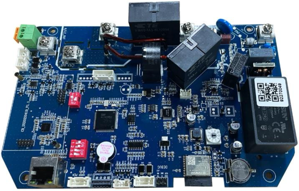
Inside these products, PCBs may control power conversion, communication, monitoring, protection, user interfaces, charging management, and other functions.
An SMT solution for EV charger PCBs therefore needs to consider more than component placement speed.
Depending on the product architecture, an EV charger PCB may combine:
- Microcontrollers and control ICs
- Communication modules
- MOSFETs or other power semiconductors
- Diodes
- Resistors and capacitors
- Transformers
- Inductors and chokes
- Relays
- Fuses
- Connectors
- Terminal blocks
- Large electrolytic capacitors
- Current or voltage sensing components
Some boards may also use thick copper, large copper areas, heavy components, or a combination of SMT and THT technologies.
The manufacturing process should consequently be designed around the PCB structure, BOM, electrical requirements, production volume, testing strategy, and product mix.
Typical EV Charger PCB Assembly Process
A typical SMT process can include:
PCB Loading → Solder Paste Printing → SPI → SMT Placement → Reflow Soldering → AOI → Programming → Electrical/Functional Testing → PCB Unloading
For mixed-technology EV charger boards, the process may be expanded to:
SMT Printing → SPI → SMT Placement → Reflow → AOI → THT Insertion → Wave/Selective Soldering → Inspection → Programming → Functional Testing
Additional processes may include:
- X-ray inspection
- PCB cleaning
- Conformal coating
- Barcode identification
- Automated material handling
- ICT
- Electrical safety testing
- Functional testing
- Traceability
- Rework
Not every EV charger PCB requires all of these processes. The final configuration should be determined by the actual product design and manufacturing requirements.
PCB and BOM Analysis Comes First
Before selecting SMT equipment, manufacturers should analyze the actual EV charger PCB.
PCB Data
Important information includes:
- PCB length and width
- Thickness
- Weight
- Number of layers
- Copper thickness
- Panel dimensions
- PCB warpage
- Large copper areas
- Heat-generating regions
Heavy copper and large copper areas can affect thermal behavior during soldering and should be considered when developing the process.
BOM Data
The BOM should be reviewed for:
- Component quantity
- Smallest package
- Largest package
- Component height
- Fine-pitch ICs
- Power semiconductors
- Inductors
- Transformers
- Electrolytic capacitors
- Relays
- Connectors
- Terminal blocks
- Fuses
- THT components
- Production Data
- Manufacturers should also define:
- Target boards per hour
- Monthly production volume
- Number of product models
- Product mix
- Number of shifts
- Expected future capacity
This information forms the basis for SMT line configuration.
Solder Paste Printing and SPI Inspection
Automatic Solder Paste Printing
For medium- and high-volume EV charger PCB production, automatic solder paste printing can provide more consistent process control than manual printing.
Key factors include:
- PCB size
- Stencil dimensions
- Board thickness
- Automatic alignment
- PCB support
- Squeegee configuration
- Paste release
- Stencil cleaning
- Printing cycle time
EV charger PCBs may contain a mixture of fine-pitch control components and larger power-related pads.
Stencil design therefore needs to account for different pad geometries and thermal characteristics.
SPI Inspection
SPI can inspect solder paste before component placement.
Typical measurements include:
- Paste volume
- Paste height
- Paste area
- Position
- Shape
This provides an opportunity to detect printing problems before component placement and reflow.
For high-reliability power electronics, early process detection can help reduce downstream rework and improve manufacturing control.
Pick and Place Equipment for EV Charger PCBs
The placement system should be selected based on the complete component mix rather than maximum theoretical speed.
Important selection criteria include:
- Placement accuracy
- Component size range
- Placement speed
- Feeder capacity
- Tray support
- Component recognition
- PCB dimensions
- Component height
- Changeover requirements
An EV charger PCB may contain hundreds of small SMT components together with larger components.
A flexible placement machine can therefore be important when the factory needs to handle different component types and multiple PCB models.
Example
Assume an EV charger PCB requires:
- 450 placements per board
- Target output: 100 boards/hour
The theoretical placement requirement is:
450 × 100 = 45,000 placements/hour
However, this does not mean a machine rated at exactly 45,000 placements/hour will necessarily achieve 100 boards/hour in production.
Actual throughput can be affected by:
- Component distribution
- Feeder arrangement
- Nozzle changes
- Component recognition
- Tray components
- PCB transfer
- Machine configuration
- Changeover
- Equipment utilization
Machine selection should therefore use actual placement data whenever possible.
Reflow Soldering for Power Electronics PCBs
Reflow soldering is one of the most important processes in EV charger PCB assembly.
Compared with small consumer-electronics boards, some EV charger PCBs may have:
- Large copper areas
- Heavy copper
- Large power components
- Large thermal pads
- Different component thermal limits
These factors can create thermal differences across the PCB.
A suitable reflow oven should provide stable and controllable thermal performance.
Important considerations include:
- Heating zones
- Cooling zones
- Conveyor width
- Temperature control
- Thermal uniformity
- PCB clearance
- Recipe management
- Nitrogen capability where required
There is no universal reflow profile for all EV charger PCBs.
The actual profile should be developed based on:
- Solder paste specifications
- PCB construction
- Copper distribution
- Component thermal mass
- Component temperature limits
- Assembly requirements
Thermal profiling using the actual PCB is therefore an important part of process setup.
AOI and X-Ray Inspection
After reflow, AOI can identify many visible assembly defects, such as:
- Missing components
- Incorrect components
- Component shift
- Incorrect orientation
- Polarity errors
- Solder bridges
- Insufficient visible solder
Other visible placement or soldering abnormalities
X-ray can provide additional inspection capability for selected hidden solder joints or structures that cannot be adequately inspected optically.
However, X-ray should not be treated as a mandatory process for every EV charger PCB.
Its use depends on:
- Component packages
- PCB design
- Customer requirements
- Process risk
- Quality strategy
Inspection technology should be selected according to the actual product rather than simply adding equipment to the line.
THT Assembly for EV Charger PCBs
EV charger boards may use both SMT and THT components.
Depending on the design, THT components can include:
- Large connectors
- Terminal blocks
- Transformers
- Inductors
- Relays
- Fuses
- Large capacitors
- Selected power components
For boards containing significant THT content, the SMT process may be followed by THT assembly.
A typical mixed-technology flow is:
SMT → Reflow → AOI → THT Insertion → Wave/Selective Soldering → Inspection → Testing
Wave Soldering
Wave soldering may be suitable when many compatible THT joints can be soldered efficiently together.
Selective Soldering
Selective soldering can be useful when only specific areas or joints require soldering, particularly when:
- Bottom-side SMT components are present
- THT joints are concentrated in specific areas
- Production is high-mix
- Wave soldering would expose unsuitable areas to molten solder
The choice should be based on actual PCB geometry and production requirements.
Electrical and Functional Testing
Testing is particularly important for EV charger electronics because assembly inspection alone cannot verify all electrical functions.
Depending on the product, testing may include:
- ICT
- Continuity testing
- Programming
- Power-on testing
- Communication testing
- Voltage measurement
- Current measurement
- Charging control verification
- Protection-function testing
- Product-specific functional testing
Safety or high-voltage testing may also be required depending on the product design and applicable requirements.
Testing requirements should be defined during production-line planning because testing can become the main capacity constraint.
Example of a Testing Bottleneck
Consider this simplified line:
Even though the SMT equipment can support significantly higher theoretical throughput, the overall production flow can be constrained by functional testing.
This is why an EV charger SMT solution should include downstream testing when calculating real production capacity.
Programming and Traceability
Many EV charger control boards require programming or configuration after assembly.
This may include:
- Firmware programming
- Product configuration
- Serial number assignment
- Communication parameter configuration
- Product identification
- Traceability can also connect production information to an individual PCB.
Depending on customer and product requirements, traceability may include:
- PCB serial number
- Product model
- PCB revision
- Production time
- Machine information
- Program version
- Material or component lot
- Solder paste information
- SPI results
- Reflow data
- AOI results
- Programming results
- Functional test results
Such data can support quality analysis and process investigation.
Conformal Coating: Is It Required?
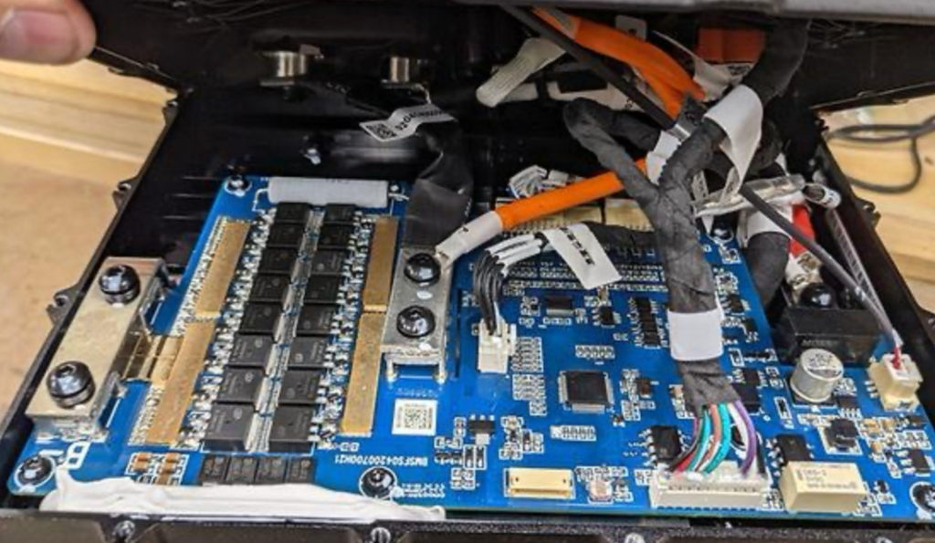
Some EV charger PCBs may operate in environments involving:
- Humidity
- Condensation
- Dust
- Temperature variation
- Other environmental exposure
Conformal coating may therefore be considered for selected applications.
However, not every EV charger PCB requires conformal coating.
The decision should consider:
- Product environment
- Enclosure design
- PCB location
- Customer specifications
- Material compatibility
- Required protection
- Repair requirements
When coating is used, areas such as connectors, test points, switches, contacts, and programming interfaces may require keep-out zones.
Selective coating equipment can help control coating placement, but automation does not necessarily eliminate every masking requirement.
High-Mix vs High-Volume EV Charger Production
Different production environments require different SMT configurations.
High-Mix Production
A high-mix factory may prioritize:
- Flexible placement machines
- Large feeder capacity
- Offline feeder preparation
- Fast changeover
- Recipe management
- Barcode identification
- Flexible material handling
A typical configuration may be:
Loader → Printer → SPI → Flexible Placement → Reflow → AOI → Programming → Functional Testing
High-Volume Production
High-volume production may prioritize:
- High placement throughput
- Multiple placement machines
- Automated material handling
- Automatic loading and unloading
- Inline inspection
- Parallel testing
- Production traceability
A possible configuration is:
Automatic Loading → Printing → SPI → Multiple Placement Machines → Reflow → AOI → Programming → Parallel Testing → Unloading
The correct solution depends on actual production data rather than whether a factory is simply classified as “high volume.”
Line Balancing and Factory Layout
A complete EV charger PCB production line should be planned as one integrated manufacturing system.
Important considerations include:
- Material Flow
- Component storage
- Kitting
- Feeder preparation
- SMT line feeding
- THT material handling
- Finished PCB handling
- Production Flow
- PCB loading
- Printing
- Placement
- Reflow
- Inspection
- THT
- Testing
- Rework
- Factory Utilities
- Power
- Compressed air
- Exhaust
- ESD protection
- Nitrogen where required
- Cooling or HVAC requirements
- Maintenance access
- Production Management
- Recipe management
- Barcode control
- Traceability
- WIP management
- Quality data
- Changeover planning
A high-speed SMT machine cannot compensate for poor material flow or an undersized testing area.
New vs Pre-Owned SMT Equipment
EV charger manufacturers can evaluate both new and pre-owned equipment depending on investment strategy.
New SMT Equipment
New equipment may be suitable when the factory requires:
- New capacity
- Modern automation
- Standardized production
- Long-term expansion
- New software and control functions
Pre-Owned Equipment
Pre-owned SMT equipment may be considered when investment control is a priority.
Before purchasing, evaluate:
- Machine condition
- Operating history
- Placement accuracy
- Feeder condition
- Software
- Spare parts
- Maintenance history
- Technical support
- Compatibility with the rest of the line
A hybrid line can also combine new and pre-owned equipment to balance investment and production capability.
Why Choose Fuliu Electronics for EV Charger SMT Solutions?
Established in 2014, Fuliu Electronics is dedicated to providing high-quality PCBA intelligent manufacturing solutions and services.
With extensive SMT industry experience, Fuliu Electronics provides equipment and services including:
- SMT production line planning
- Pick and place machines
- Automatic solder paste printers
- ERSA reflow ovens from Germany
- MagicRay SPI and AOI inspection systems
- SMT equipment leasing
- SMT equipment maintenance
- Pre-owned SMT equipment
- SMT spare parts
- Complete SMT production line solutions
Fuliu Electronics works with leading SMT equipment brands including Fuji, Panasonic, ASM, Yamaha, JUKI, and Hanwha.
For EV charger PCB manufacturing, equipment selection should be based on PCB dimensions, component mix, placement requirements, thermal characteristics, THT content, testing requirements, production volume, and future expansion.
Fuliu Electronics can integrate these factors into an overall SMT production line solution instead of treating each machine as an independent purchase.
The company is also expanding its international business across India, Vietnam, the Philippines, Indonesia, the Middle East, South Africa, and Europe.
Frequently Asked Questions
A typical SMT line includes an automatic solder paste printer, SPI, pick and place machine, reflow oven, AOI, PCB handling equipment, and downstream testing. THT equipment may be added depending on the PCB design.
EV charger PCBs may contain large copper areas, power components, heavy components, and mixed SMT/THT assemblies. Thermal management and electrical testing can therefore require additional process planning.
SPI is not universally mandatory, but it can provide useful control over solder paste deposition and identify printing problems before component placement.
SMT components are generally reflow soldered, but the exact process depends on the PCB design and assembly technology. THT components may require wave or selective soldering afterward.
The decision depends on THT joint quantity, PCB layout, bottom-side SMT components, production volume, and soldering accessibility. Neither process is universally better.
AOI can detect many visible assembly defects, but it does not replace electrical or functional testing. X-ray may also be considered for selected hidden solder joints.