
Wave soldering is one of the most established soldering processes used in through-hole PCB assembly.
It is commonly used to solder components such as:
- Connectors
- Terminal blocks
- Relays
- Transformers
- Switches
- Pin headers
- Large capacitors
- Selected power components
During wave soldering, a PCB passes through a controlled production process that typically includes flux application, preheating, contact with a molten solder wave, and cooling.
The component leads protruding through the underside of the PCB contact the solder wave, allowing many through-hole joints to be soldered during one continuous pass.
A typical production flow is:
THT Component Insertion → Pre-Solder Inspection → Fluxing → Preheating → Wave Soldering → Cooling → Inspection → Testing
Wave soldering is therefore an important part of many DIP/THT production lines.
However, achieving stable soldering quality requires much more than simply passing a PCB over molten solder.
PCB design, component solderability, flux application, preheating, solder temperature, conveyor speed, wave condition, board orientation, and machine maintenance can all influence the final solder joints.
What Is Wave Soldering?
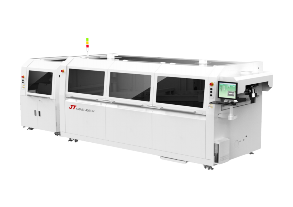
Wave soldering is a process in which the underside of a PCB passes over a continuously circulating wave of molten solder.
Through-hole component leads extend through plated holes in the PCB.
When the board contacts the solder wave, molten solder wets the exposed component leads and PCB pads.
After the PCB leaves the solder wave, the solder cools and solidifies.
This creates electrical and mechanical connections between the components and PCB.
Wave soldering is most closely associated with THT, or Through-Hole Technology, although certain specialized processes have also historically used wave soldering with surface-mount components.
In modern production, however, SMT components are primarily soldered using reflow soldering.
Why Is It Called “Wave” Soldering?
The name comes from the molten solder wave generated inside the soldering machine.
Rather than dipping the entire PCB into a static solder bath, a pump creates a controlled upward wave of molten solder.
The PCB moves over this wave on a conveyor.
Only the required underside area makes contact with the solder under controlled process conditions.
The wave shape, height, stability, and contact conditions can influence soldering quality.
What Is Wave Soldering Used For?
Wave soldering is primarily used for through-hole components.
Typical applications include:
- Industrial control PCBs
- Power supply boards
- Automotive electronic modules
- Home appliance control boards
- Energy equipment
- Communication systems
- Factory automation
- Consumer electronics containing THT parts
It is particularly useful when a board contains many through-hole joints that can be soldered efficiently in one continuous production process.
What Components Are Commonly Wave Soldered?
Common wave-soldered THT components can include:
Connectors
Examples include:
- Multi-pin connectors
- Headers
- Power connectors
- Communication connectors
Terminal Blocks
These are widely used in:
- Industrial control
- Power electronics
- Automation equipment
- Energy systems
Relays
Through-hole relays are common in control and switching applications.
Transformers
Transformers are often relatively large components and may use through-hole leads.
Capacitors
Large radial or electrolytic capacitors are frequently assembled using THT.
Switches
Some switches and electromechanical components use through-hole mounting.
Selected Power Components
Some power devices are still supplied in through-hole packages depending on the application.
How Does the Wave Soldering Process Work?
A complete wave soldering process includes several stages.
Step 1: THT Component Insertion
Before soldering, through-hole components must be inserted into the PCB.
Insertion can be:
- Manual
- Semi-automatic
- Automatic
The correct method depends on:
- Component type
- Geometry
- Packaging
- Production volume
- Automation requirements
Many DIP/THT lines use a combination of automatic and manual insertion.
For example, standardized components may be automatically inserted while large or irregular components remain manual.
Step 2: Pre-Solder Inspection
Before the PCB enters the wave soldering machine, the assembly should be checked.
Typical inspection points include:
- Missing components
- Incorrect components
- Wrong polarity
- Wrong orientation
- Bent leads
- Incorrect insertion depth
- Loose components
Detecting insertion problems before soldering can reduce post-solder rework.
Step 3: Flux Application
Flux is applied to the solder side of the PCB.
Modern wave soldering machines commonly use spray fluxing systems.
Flux supports soldering by helping prepare the metal surfaces for wetting.
The flux process should control:
- Application quantity
- Coverage
- Spray width
- Uniformity
- Conveyor synchronization
Too little flux can contribute to poor wetting.
Too much flux may create unnecessary residues or process instability depending on the flux chemistry and application.
Step 4: Preheating
After fluxing, the PCB enters the preheating section.
Preheating is important because it can:
- Activate the flux
- Gradually raise PCB temperature
- Reduce sudden thermal changes
- Support stable solder wetting
- Help manage moisture and solvent evaporation according to the process
The correct preheat conditions depend on:
- PCB thickness
- Copper distribution
- Component thermal mass
- Flux chemistry
- Solder alloy
- Conveyor speed
There is no single universal preheat temperature suitable for every PCB.
Step 5: Contact with the Solder Wave
After preheating, the PCB passes over the molten solder wave.
The solder contacts:
- THT component leads
- PCB pads
- Plated through-holes
The process should provide enough contact to create proper solder joints without causing excessive soldering defects.
Important process factors include:
- Solder temperature
- Conveyor speed
- Wave height
- Contact time
- PCB angle
- Board orientation
- Solder wave stability
Step 6: Cooling
After leaving the solder wave, the PCB begins to cool.
Cooling helps the molten solder solidify before downstream inspection and handling.
Depending on the line configuration, cooling may be integrated into the wave soldering machine or performed on a downstream cooling conveyor.
Step 7: Post-Solder Inspection
The PCB should then be inspected for soldering quality.
Typical inspection targets include:
- Solder bridges
- Insufficient solder
- Poor wetting
- Incomplete hole fill
- Icicles
- Solder balls
- Excessive solder
Inspection methods can include:
- Visual inspection
- Magnification
- AOI where suitable
- X-ray for selected structures
Step 8: Electrical and Functional Testing
After soldering inspection, the PCBA may proceed to testing.
Depending on the product, testing can include:
- ICT
- Functional testing
- Power-on testing
- Programming
- Communication testing
- I/O testing
Testing should be included when calculating total production line capacity.
Main Sections of a Wave Soldering Machine
A modern wave soldering machine usually combines several process modules.
Fluxing System
The fluxing system applies flux to the PCB underside.
Spray fluxing is commonly used because application can be controlled according to PCB width and conveyor movement.
Preheating Section
Preheating may use different heating technologies depending on machine design.
The objective is to achieve suitable board and flux conditions before solder contact.
Conveyor System
The conveyor transports the PCB through the machine.
Important conveyor characteristics include:
- Speed stability
- Width adjustment
- Board support
- Transport angle
- Production compatibility
Solder Pot
The solder pot contains the molten solder alloy.
Temperature and solder condition must be controlled and maintained.
Wave System
The pumping system creates the solder wave.
Machine designs may use different wave configurations depending on process requirements.
Cooling Section
Cooling helps stabilize the assembly after soldering.
Control System
Modern machines can provide control for:
- Conveyor speed
- Preheat settings
- Solder temperature
- Fluxing parameters
- Recipes
- Production monitoring
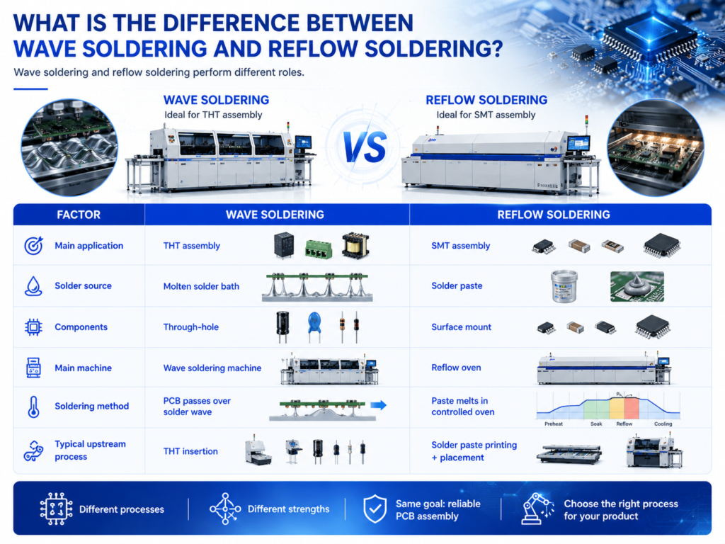
What Is the Difference Between Wave Soldering and Reflow Soldering?
Wave soldering and reflow soldering perform different roles.
In a mixed SMT/THT PCB assembly process, both may be used.
A typical flow is:
Solder Paste Printing → SPI → SMT Placement → Reflow → AOI → THT Insertion → Wave Soldering → Inspection → Testing
What Is the Difference Between Wave Soldering and Selective Soldering?
Both are used for through-hole assembly, but the way solder is applied differs.
Wave Soldering
A broader area of the PCB underside passes over a molten solder wave.
This can be efficient when many THT joints need to be soldered.
Selective Soldering
Only programmed joints or areas are exposed to solder.
This can be useful when:
- Only a few THT components are present
- Bottom-side SMT components restrict wave contact
- PCB geometry is complex
- Specific regions need to avoid solder
The correct choice depends on PCB design and production requirements.
When Should You Use Wave Soldering?
Wave soldering may be a suitable choice when:
- The PCB contains many through-hole joints
- Production volume is medium or high
- The solder side supports wave contact
- Continuous production is required
- The product benefits from efficient multi-joint soldering
It is especially useful for boards with multiple:
- Connectors
- Terminal blocks
- Relays
- Headers
- Transformers
When May Wave Soldering Not Be the Best Choice?
Wave soldering may be less suitable when:
- Only a few THT joints are present
- Bottom-side SMT components create clearance issues
- Certain areas must avoid solder contact
- PCB geometry limits wave access
- The product is a prototype or very small batch
In these cases, selective or manual soldering may be considered.
Common Wave Soldering Defects
Stable wave soldering requires careful process control.
Several defects can occur when process conditions are not optimized.
Solder Bridges
A solder bridge forms when solder creates an unwanted connection between adjacent pads or leads.
Possible contributing factors include:
- Conveyor speed
- Wave contact
- Lead spacing
- PCB orientation
- Solderability
- Flux conditions
Insufficient Solder
A joint may not receive enough solder.
Possible causes can include:
- Poor wetting
- Inadequate flux
- Insufficient contact time
- Contaminated surfaces
- Process settings
Poor Wetting
Poor wetting occurs when solder does not properly spread across the required metal surfaces.
Possible factors include:
- Oxidation
- Component condition
- PCB finish
- Flux selection
- Preheat
- Solder condition
Incomplete Hole Fill
The solder may fail to fill the plated through-hole to the required level.
Potential factors include:
- High thermal mass
- Insufficient flux activity
- Inadequate preheat
- Limited solder contact
- Lead-to-hole geometry
- Solderability
Icicles
Sharp solder projections can form as the PCB exits the wave.
Potential factors may include:
- Exit conditions
- Solder temperature
- Conveyor speed
- Flux activity
- Wave stability
Solder Balls
Small solder particles may appear on the PCB.
Potential causes can involve:
- Flux
- Moisture
- Mask condition
- Preheat
- Soldering dynamics
Defect troubleshooting should consider the entire process rather than adjusting one parameter in isolation.
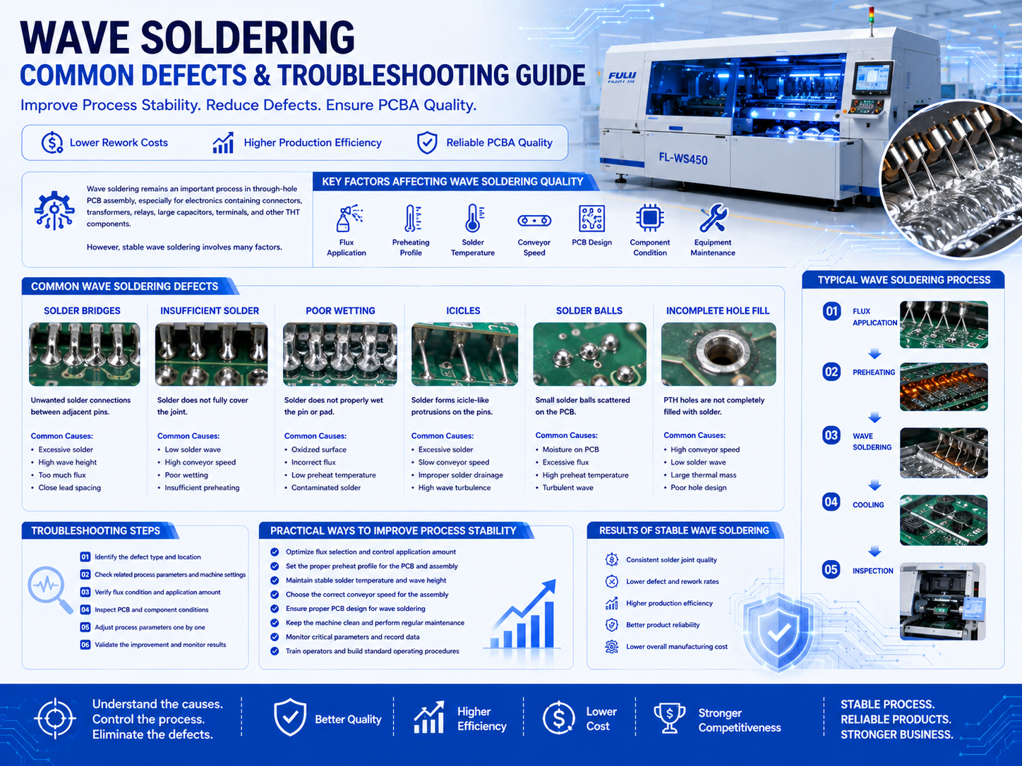
What Parameters Affect Wave Soldering Quality?
Several variables interact with one another.
Important parameters include:
- Flux type
- Flux quantity
- Preheat profile
- Solder alloy
- Solder temperature
- Conveyor speed
- Wave height
- Contact time
- PCB angle
- PCB orientation
- Component lead condition
- PCB solderability
- Machine cleanliness
This is why copying process settings from another product does not guarantee good results.
Each PCB should be evaluated according to its own thermal and soldering requirements.
Is There a Standard Wave Soldering Temperature?
There is no single temperature setting that is correct for every product.
The appropriate solder temperature depends on:
- Solder alloy
- Flux
- PCB construction
- Component specifications
- Process requirements
- Conveyor conditions
Manufacturers should establish a validated process window for the specific product and materials being used.
Why Is PCB Orientation Important?
PCB orientation can influence how solder drains away from component leads and pads.
Poor orientation can contribute to bridging or other defects in certain layouts.
When planning wave soldering, process engineers should consider:
- Lead direction
- Component spacing
- Pad arrangement
- Dense connector areas
- Board geometry
In some cases, rotating the PCB relative to the wave can improve process behavior.
Does Wave Soldering Require a Pallet?
Not always.
A solder pallet may be used when:
- Certain areas need protection
- Bottom-side SMT components need shielding
- PCB support is required
- Board geometry requires controlled exposure
However, pallet use adds:
- Tooling cost
- Maintenance
- Cleaning
- Thermal mass
The need for a pallet should therefore be evaluated during process planning.
What Is the Role of PCB Design in Wave Soldering?
Good wave soldering starts with manufacturable PCB design.
Important factors may include:
- Pad dimensions
- Hole size
- Lead spacing
- Component spacing
- Board orientation
- Bottom-side clearance
- Solder mask design
- Thermal connections
Design-for-manufacturing review can reduce production difficulties before the PCB enters mass production.
How to Improve Wave Soldering Stability
Manufacturers can improve process stability by focusing on the whole production system.
Useful practices include:
- Control PCB and component solderability
- Maintain consistent flux application
- Establish suitable preheat conditions
- Monitor solder temperature
- Control conveyor speed
- Maintain wave stability
- Clean the machine regularly
- Monitor solder condition
- Inspect nozzles and pumps
- Standardize recipes
- Analyze defects systematically
- Train operators and technicians
Process changes should be based on evidence from actual boards and inspection data.
How Wave Soldering Fits Into a DIP Production Line
A complete DIP/THT line can look like:
PCB Loader → Component Preparation → THT Insertion → Pre-Solder Inspection → Wave Soldering → Cooling Conveyor → PCB Unloader → Inspection → Testing
Supporting equipment may include:
- Lead cutting machines
- Component forming equipment
- Insertion conveyors
- ESD workstations
- Fume extraction
- Rework stations
The exact line should be configured according to the PCB and BOM.
Manual vs Semi-Automatic vs Automatic Wave Soldering Line
Wave soldering can be used in production lines with different automation levels.
Manual THT Line
Suitable for:
- Low-volume production
- Prototypes
- High product mix
Operators may manually load boards, insert components, and transfer PCBs.
Semi-Automatic Line
A typical configuration may include:
Automatic Loader → Insertion Conveyor → Manual THT Insertion → Wave Soldering → Cooling → Unloader
This reduces PCB handling while maintaining component insertion flexibility.
Highly Automated Line
A more automated line may use:
Automatic Loader → Automatic/Semi-Automatic THT Insertion → Inspection → Automatic Transfer → Wave Soldering → Cooling → Automated Inspection → Testing → Unloader
The correct level depends on production economics.
How to Calculate Wave Soldering Line Capacity
Rated machine speed alone does not determine factory output.
Suppose:
- THT insertion: 40 boards/hour
- Wave soldering: 75 boards/hour
- Inspection: 50 boards/hour
- Functional testing: 30 boards/hour
The practical finished output cannot exceed the effective capacity of the bottleneck process.
In this example, testing may limit output to around 30 boards per hour unless the testing process is improved or additional test capacity is added.
This is why the entire line should be balanced.
How to Choose a Wave Soldering Machine
Before selecting a machine, manufacturers should provide:
- PCB length and width
- PCB thickness
- Panel dimensions
- BOM
- THT component list
- Maximum component height
- Bottom-side PCB layout
- Solder alloy
- Flux requirements
- Target production capacity
- Product mix
- Changeover frequency
- Required process flexibility
- Factory layout
- Available utilities
- Existing equipment
- Inspection and testing requirements
- Budget
The machine should be selected for the real production requirement rather than simply choosing the largest available model.
New vs Pre-Owned Wave Soldering Equipment
Both new and suitable pre-owned equipment can be considered.
New Equipment
Potential advantages include:
- New machine condition
- Current-generation control functions
- Warranty options
- Long-term platform planning
Pre-Owned Equipment
Potential advantages can include:
- Lower initial investment
- Faster capacity expansion
- Access to established equipment platforms
When evaluating a pre-owned wave soldering machine, check:
- Solder pot condition
- Pump and wave system
- Conveyor
- Fluxing system
- Preheating system
- Control electronics
- Maintenance history
- Spare parts availability
- Technical support
The decision should be based on total cost of ownership and process compatibility.
Wave Soldering and PCBA Production Line Solutions from Fuliu Electronics
Established in 2014, Fuliu Electronics is dedicated to providing customers with high-quality PCBA intelligent manufacturing solutions and services.
With extensive experience in the SMT industry, we specialize in dependable equipment, professional technical support, and complete SMT and PCBA production line solutions.
Our product portfolio includes SMT pick and place machines from Fuji, Panasonic, ASM, Yamaha, JUKI, and Hanwha, together with ERSA reflow ovens from Germany, MagicRay SPI/AOI inspection systems, automatic solder paste printers, supporting PCBA equipment, pre-owned SMT equipment, SMT spare parts, machine leasing, and maintenance services.
For customers planning or upgrading a wave soldering line, Fuliu Electronics can help evaluate:
- PCB dimensions
- BOM
- THT component types
- Target production capacity
- Product mix
- Wave vs selective soldering
- Component insertion method
- Inspection and testing
- Existing equipment
- Factory layout
- Automation level
- Investment budget
For mixed SMT + THT products, the entire process can also be evaluated as one complete PCBA manufacturing system.
As part of our global growth strategy, Fuliu Electronics is actively expanding into international markets, with key focus areas including India, Vietnam, the Philippines, Indonesia, the Middle East, South Africa, and Europe.
Conclusion
So, what is wave soldering in PCB assembly?
Wave soldering is a production process mainly used to solder through-hole components by passing the underside of a PCB over a controlled wave of molten solder.
A typical process is:
THT Insertion → Inspection → Fluxing → Preheating → Solder Wave → Cooling → Inspection → Testing
Wave soldering can be particularly effective when:
- Many THT joints are present
- The PCB design supports wave contact
- Medium- or high-volume production is required
- Continuous production flow is important
However, good soldering quality depends on much more than the solder wave itself.
Manufacturers must control:
- Flux
- Preheating
- Solder temperature
- Conveyor speed
- Wave stability
- PCB design
- Component solderability
- Machine maintenance
For PCBs containing only a limited number of THT joints or complex bottom-side SMT components, selective soldering may be a more suitable alternative.
If you are planning a new wave soldering line, upgrading an existing DIP/THT production process, or building a complete SMT + THT PCBA factory, Fuliu Electronics can help evaluate your PCB dimensions, BOM, THT component mix, target capacity, existing equipment, factory layout, automation requirements, and budget to develop a suitable production solution.
Frequently Asked Questions
Lorem ipsum dolor sit amet, consectetur adipiscing elit, sed do eiusmod tempor incididunt ut labore et dolore magna aliqua. Ut enim ad minim veniam, quis nostrud exercitation.
Common examples include connectors, terminal blocks, relays, transformers, pin headers, switches, large capacitors, and selected power components.
In modern PCB manufacturing, wave soldering is primarily used for THT assembly, while SMT components are normally soldered using reflow.
The main stages are fluxing, preheating, solder-wave contact, cooling, and inspection.
Reflow soldering melts solder paste to solder surface-mount components, while wave soldering uses molten solder to process through-hole joints.
Wave soldering processes a broader underside area, while selective soldering targets programmed THT joints or areas.