
Through-hole technology remains an important part of modern electronics manufacturing, even as Surface Mount Technology (SMT) has become the dominant assembly method for many electronic products.
Connectors, transformers, relays, power components, large capacitors, switches, terminals, and other components are still frequently assembled using Through-Hole Technology (THT) because of their mechanical strength, electrical characteristics, and suitability for demanding applications.
However, through-hole PCB assembly introduces its own quality challenges.
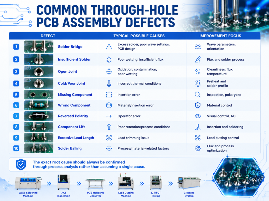
Common defects such as solder bridges, insufficient solder, poor wetting, missing components, reversed polarity, lifted components, and excessive lead length can reduce first-pass yield and increase rework costs.
The good news is that most through-hole PCB assembly defects can be reduced through systematic process control.
This guide explains the most common THT/DIP assembly defects, their possible causes, and practical ways manufacturers can improve component insertion, wave soldering, inspection, testing, and overall production quality.
What Is Through-Hole PCB Assembly?
Through-hole PCB assembly is a manufacturing process in which component leads are inserted through holes in a printed circuit board and soldered to pads on the opposite side.
A typical process may include:
Component Preparation → Component Insertion → Pre-Solder Inspection → Flux Application → Preheating → Wave/Selective Soldering → Cooling → Lead Processing → AOI/Visual Inspection → ICT/FCT → Rework → Final Inspection
Through-hole assembly is also commonly called:
- THT assembly
- DIP assembly
- Through-hole insertion
- DIP production
Although “DIP” technically refers to Dual In-line Package, many electronics factories use the term more broadly when referring to through-hole production lines.
Why Do Defects Occur in Through-Hole PCB Assembly?
THT assembly quality depends on several processes working together.
Defects can originate from:
- Incorrect component preparation
- Manual insertion errors
- PCB contamination
- Poor flux application
- Incorrect preheating
- Unstable solder temperature
- Incorrect conveyor speed
- Improper wave height
- PCB design limitations
- Poor equipment maintenance
- Insufficient inspection
- Operator inconsistency
This means improving quality requires more than adjusting the wave soldering machine.
Manufacturers need to control the complete DIP/THT production process.
Common Through-Hole PCB Assembly Defects
The exact root cause should always be confirmed through process analysis rather than assuming a single cause.
Prevent Incorrect Component Insertion
Component insertion is one of the most important quality-control stages in a DIP production line.
Manual insertion can create errors such as:
- Missing components
- Wrong components
- Reversed polarity
- Incorrect orientation
- Components inserted into the wrong position
- Components not fully seated
These defects become more expensive to correct after soldering.
How to Reduce Insertion Errors
Use standardized work instructions that clearly show:
- Component position
- Part number
- Polarity
- Orientation
- Insertion sequence
Factories can also use:
- Color-coded material trays
- Component identification systems
- Dedicated fixtures
- Barcode verification
- Pick-to-light systems
- Camera-assisted workstations
The goal is to detect or prevent mistakes before the PCB reaches wave soldering.
Control Component Lead Preparation
Some through-hole components require lead forming or cutting before insertion.
Poor preparation can cause:
- Incorrect lead spacing
- Damaged components
- Poor component seating
- Excessive mechanical stress
- Difficult insertion
Lead-forming equipment should therefore be properly adjusted according to component and PCB specifications.
Operators should avoid excessive bending close to the component body where it could damage the component.
Improve PCB and Component Solderability
Good solder joints require solderable surfaces.
Oxidation, contamination, poor storage, or aging can negatively affect solder wetting.
Manufacturers should control:
- PCB storage
- Component storage
- Moisture exposure where relevant
- Surface contamination
- Material shelf life
- Incoming material quality
If solderability problems occur repeatedly, investigate the PCB finish and component leads rather than compensating only by changing soldering parameters.
Optimize Flux Application
Flux plays an important role in wave soldering.
It helps remove surface oxides and supports proper solder wetting.
Incorrect flux application can contribute to:
- Insufficient solder
- Poor wetting
- Open joints
- Excess residue
- Soldering instability
Important parameters can include:
- Flux type
- Application volume
- Spray uniformity
- Flux density or solids content where applicable
- Conveyor speed
More flux is not necessarily better.
The goal is controlled and consistent application.
Control the Preheating Process
After flux application, the PCB normally passes through preheating before contacting the solder wave.
Preheating can help:
- Activate flux
- Reduce thermal shock
- Remove volatile components
- Prepare the assembly for soldering
Insufficient or excessive preheating can both create problems.
Manufacturers should develop and verify a thermal profile based on:
- PCB thickness
- Board mass
- Component density
- Flux chemistry
- Solder alloy
- Component temperature limitations
Actual board temperatures should be measured rather than relying only on machine setpoints.
Optimize Wave Soldering Temperature
Solder temperature has a major influence on wetting and joint formation.
If process temperatures are unsuitable, defects may include:
- Poor wetting
- Insufficient solder
- Thermal damage
- Excessive oxidation
- Unstable solder joints
However, there is no universal temperature that is correct for every PCB.
The appropriate process depends on:
- Solder alloy
- Flux chemistry
- PCB construction
- Component requirements
- Conveyor speed
- Contact time
Process settings should be validated using the materials and products actually being manufactured.
Adjust Conveyor Speed and Contact Time
The PCB must interact with the solder wave for an appropriate amount of time.
If conveyor speed is too high, there may be insufficient contact for reliable joint formation.
If it is too slow, excessive thermal exposure or solder-related problems may occur.
Manufacturers should therefore optimize:
Conveyor Speed + Wave Height + Contact Time + Solder Temperature
as a complete process rather than adjusting each parameter independently.
Reduce Solder Bridges
A solder bridge occurs when solder unintentionally connects adjacent conductive areas.
This can create an electrical short circuit.
Potential contributing factors include:
- Excessive wave contact
- Incorrect conveyor settings
- Poor PCB orientation
- Inadequate solder drainage
- Component lead geometry
- PCB design
- Flux/process problems
How to Reduce Solder Bridges
Possible improvements include:
- Optimizing conveyor speed
- Adjusting wave height
- Reviewing PCB travel direction
- Improving flux control
- Checking lead length
- Reviewing pad and component layout
For recurring bridging on the same PCB locations, a design-for-manufacturing (DFM) review may be necessary.
Prevent Insufficient Solder
Insufficient solder can result in weak or unreliable joints.
Possible causes include:
- Poor solderability
- Insufficient flux
- Incorrect preheat
- Contaminated surfaces
- Inadequate wave contact
- Poor hole fill
To reduce insufficient solder:
- Verify PCB and component cleanliness
- Check flux application
- Confirm the thermal profile
- Inspect solderability
- Optimize wave contact
- Review hole-to-lead relationships
Repeated insufficient solder should be treated as a process problem requiring root-cause analysis.
Improve Through-Hole Fill
For plated through-hole assemblies, solder should properly wet and fill the required joint area according to the product’s quality criteria.
Poor barrel fill may be influenced by:
- High thermal mass
- Insufficient heating
- Poor solderability
- Contamination
- Incorrect lead-to-hole relationship
Heavy components and ground planes can absorb significant heat.
In these cases, thermal profiling becomes particularly important.
Control Component Lead Length
Lead length affects both manufacturing quality and finished PCB clearance.
Leads that are too long may:
- Increase short-circuit risk
- Interfere with enclosures
- Affect downstream assembly
Leads cut too short can potentially compromise joint integrity depending on the design.
A properly configured PCB lead cutting machine can improve consistency in high-volume production.
Use Selective Soldering for Complex PCB Designs
Traditional wave soldering is not ideal for every mixed-technology PCB.
Modern PCBAs may contain SMT components close to through-hole joints.
In these situations, selective soldering may provide greater process control.
Selective soldering applies solder to specific locations rather than exposing a broad PCB area to a solder wave.
It can be useful for:
- Mixed SMT/THT assemblies
- Complex PCB layouts
- Low THT component counts
- High-value PCBAs
- Products requiring controlled solder application
The correct process should be selected based on PCB design and production volume.
Add Pre-Solder Inspection
Finding a component insertion error before soldering is usually much cheaper than repairing it afterward.
A pre-solder inspection stage can check:
- Component presence
- Part number
- Orientation
- Polarity
- Seating
- Insertion quality
Depending on production volume, this can be performed using:
- Manual inspection
- Camera-assisted inspection
- Automated inspection
Prevention is usually more cost-effective than rework.
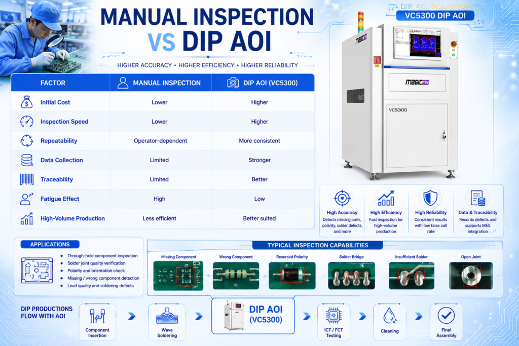
Use AOI After Wave Soldering
Automated Optical Inspection can help manufacturers identify visible assembly and soldering defects after the soldering process.
A DIP AOI system may inspect for issues such as:
- Missing components
- Incorrect polarity
- Component displacement
- Solder bridges
- Insufficient solder
- Certain visible solder anomalies
AOI provides several benefits:
- More consistent inspection
- Faster defect detection
- Reduced dependence on manual inspection
- Production data collection
- Better defect traceability
However, AOI should complement process control rather than replace it.
Use ICT and FCT for Electrical Quality Control
Visual inspection cannot identify every electrical defect.
Manufacturers may use:
ICT — In-Circuit Test
ICT can help detect:
- Shorts
- Opens
- Incorrect component values
- Circuit connectivity problems
FCT — Functional Circuit Test
FCT verifies whether the assembled PCB performs its intended functions.
Combining visual inspection, AOI, ICT, and FCT creates a more comprehensive quality-control strategy.
Maintain the Wave Soldering Machine
Poor equipment condition can gradually increase process variation.
Preventive maintenance should include appropriate checks of:
- Flux spray system
- Nozzles
- Conveyor
- Preheating system
- Solder pot
- Wave generation system
- Sensors
- Cooling system
- Exhaust
- Control systems
Maintenance frequency should be based on machine recommendations and actual production conditions.
Do not wait for a machine failure before performing maintenance.
Monitor Solder Pot Condition
Wave soldering processes require control of solder condition.
Depending on the solder alloy and production process, manufacturers may need to monitor:
- Contamination
- Dross formation
- Alloy composition
- Solder level
Poor solder-pot management can contribute to process instability.
A documented monitoring and maintenance procedure helps maintain consistent soldering performance.
Improve Operator Training
Even highly automated DIP lines still depend on skilled operators and technicians.
Training should cover:
- Component identification
- Polarity recognition
- ESD requirements
- Insertion standards
- Solder defect recognition
- Equipment operation
- Process parameter control
- Maintenance procedures
- Quality escalation
Standardized training reduces variation between shifts and operators.
Track Defect Data Instead of Only Repairing Boards
A factory that only repairs defective PCBAs without analyzing the data will repeatedly experience the same problems.
Track indicators such as:
- First-Pass Yield (FPY)
- Defects per board
- Solder bridge rate
- Insufficient solder rate
- Missing component rate
- Polarity error rate
- Rework rate
- Equipment downtime
Then classify defects by:
Machine + Product + Shift + Process + Defect Type
This makes recurring patterns easier to identify.
Use Root-Cause Analysis
When a defect repeatedly occurs, avoid simply adjusting random machine parameters.
A structured root-cause investigation can examine:
Material → Machine → Method → Manpower → Measurement → Environment
For example, repeated poor solder wetting might be related to:
- PCB oxidation
- Component lead condition
- Flux application
- Preheating
- Solder temperature
- Contamination
Finding the real cause prevents unnecessary process changes.
Recommended Quality-Control Flow for THT Assembly
A well-controlled production process can be organized as:
Incoming Material Inspection → Component Preparation → Controlled Insertion → Pre-Solder Inspection → Flux Control → Thermal Profiling → Wave/Selective Soldering → AOI → ICT/FCT → Rework Analysis → Final Inspection
Each stage acts as a quality gate.
The objective is to prevent defects from moving downstream.
How to Improve First-Pass Yield in DIP Production
First-Pass Yield measures how many PCBAs pass the manufacturing process without requiring repair or rework.
To improve FPY:
- Standardize component insertion.
- Improve material traceability.
- Optimize flux application.
- Validate preheating profiles.
- Control wave soldering parameters.
- Add appropriate inspection points.
- Maintain equipment regularly.
- Train operators.
- Analyze defect trends.
- Correct root causes instead of relying on rework.
Higher FPY can reduce labor, improve throughput, and lower manufacturing cost.
Manual Inspection vs DIP AOI
Manual inspection remains useful, particularly for complex or unusual defects, but AOI can provide substantial advantages for scalable production.
How Production Line Design Affects Defect Rate
Quality is also influenced by factory and line design.
A poorly configured DIP line may create:
- Excessive PCB handling
- Operator congestion
- Incorrect material flow
- Long waiting times
- Poor inspection positioning
- Line imbalance
A properly planned production line should consider:
- Operator ergonomics
- Material supply
- PCB flow
- Inspection locations
- Equipment capacity
- Buffer requirements
- Rework routing
This is why production line integration is an important part of quality improvement.
SMT and THT Quality Should Be Managed Together
Many PCBAs combine both SMT and through-hole components.
A typical process may be:
Solder Paste Printing → SPI → Pick and Place → Reflow → AOI → THT Insertion → Wave/Selective Soldering → DIP AOI → ICT/FCT → Cleaning → Conformal Coating
A defect created during SMT can affect downstream DIP processes, and a poor THT process can damage an otherwise good SMT assembly.
Manufacturers should therefore treat the complete PCBA line as one integrated quality system.
Why Choose Fuliu Electronics?
Established in 2014, Fuliu Electronics is dedicated to providing customers with high-quality PCBA intelligent manufacturing solutions and professional technical services.
With extensive experience in the SMT industry, we specialize in dependable equipment, technical support, and complete PCBA production line solutions.
Our equipment portfolio includes SMT pick and place machines from internationally recognized brands such as Fuji, Panasonic, ASM, Yamaha, JUKI, and Hanwha, together with ERSA reflow ovens from Germany, MagicRay SPI/AOI inspection systems, automatic solder paste printers, high-quality pre-owned SMT equipment, SMT spare parts, equipment leasing, and maintenance services.
For DIP/THT production, Fuliu Electronics can support customers with:
- DIP insertion conveyors
- Through-hole assembly workstations
- Component preparation equipment
- Wave soldering machines
- Selective soldering solutions
- DIP AOI inspection
- PCB handling and conveyor systems
- ICT/FCT integration
- PCB cleaning solutions
- Conformal coating lines
- Production line automation
- Factory layout planning
- Installation and commissioning
- Operator training
- Maintenance and technical support
Rather than focusing on an individual machine, our team can evaluate the customer’s PCB design, component types, defect problems, required capacity, existing equipment, factory layout, automation requirements, and budget to recommend a more complete production solution.
Fuliu Electronics is actively expanding into international markets, with key focus areas including India, Vietnam, the Philippines, Indonesia, the Middle East, South Africa, and Europe.
Conclusion
Reducing through-hole PCB assembly defects requires controlling the entire production process rather than relying on final inspection.
Component preparation, insertion accuracy, PCB cleanliness, flux application, preheating, wave soldering parameters, equipment maintenance, AOI, electrical testing, and operator training all influence final product quality.
A strong quality strategy follows a simple principle:
Prevent → Detect → Analyze → Improve
Prevent defects through standardized processes. Detect them as early as possible. Analyze recurring problems using production data. Then improve the process based on the actual root cause.
For manufacturers operating medium- or high-volume DIP/THT production, combining stable wave or selective soldering processes with AOI, ICT/FCT, preventive maintenance, and production data analysis can improve first-pass yield while reducing rework and manufacturing costs.
Ultimately, the best DIP production line is not simply the fastest line—it is the line that can repeatedly produce high-quality PCBAs with stable processes and predictable output.
Frequently Asked Questions
Common defects include solder bridges, insufficient solder, poor wetting, open joints, missing components, reversed polarity, component lifting, and incorrect lead length.
Control PCB and component solderability, flux application, preheating, solder temperature, conveyor speed, wave height, contact conditions, and equipment maintenance. Recurring defects should be investigated through root-cause analysis.
Possible causes include poor solderability, contamination, insufficient flux, unsuitable preheating, inadequate wave contact, and PCB/component design factors.
Optimize conveyor speed, wave conditions, PCB orientation, flux application, lead length, and process settings. If bridges repeatedly occur at the same locations, review PCB design and component layout.
Yes. Suitable DIP/THT AOI systems can inspect component presence, polarity, placement, and a range of visible soldering defects. Inspection capability depends on the equipment and PCB design.
Neither is universally better. Wave soldering is efficient for many through-hole joints and high-volume production, while selective soldering can be more suitable for complex mixed SMT/THT assemblies or PCBs with fewer through-hole joints.