
In modern SMT (Surface Mount Technology) manufacturing, quality control is no longer optional—it is a critical factor that directly impacts production yield, manufacturing costs, and customer satisfaction.
As electronic products become smaller, more complex, and more densely populated with components, PCB assembly defects can be increasingly difficult to detect and costly to repair. A single solder paste printing issue can lead to hundreds of defective boards if left unnoticed.
To prevent such problems, SMT manufacturers rely heavily on inspection systems. Among the most important technologies are SPI (Solder Paste Inspection) and AOI (Automatic Optical Inspection).
Many factory owners, process engineers, and procurement managers ask:
“AOI vs SPI: Which inspection system is more important?”
The reality is that AOI and SPI serve different purposes and work together to create a complete quality control strategy.
This article explains the key differences between AOI and SPI inspection, how each system works, and how manufacturers can select the right inspection solution for their SMT production lines.
What Is SPI Inspection?
Definition of SPI
SPI stands for Solder Paste Inspection.
It is an inspection process performed immediately after solder paste printing and before component placement.
The purpose of SPI is to verify that the correct amount of solder paste has been deposited on every PCB pad.
Position in the SMT Process
PCB Loader
↓
Solder Paste Printer
↓
SPI Inspection
↓
Pick and Place
↓
Reflow Soldering
SPI acts as the first quality gate in SMT production.
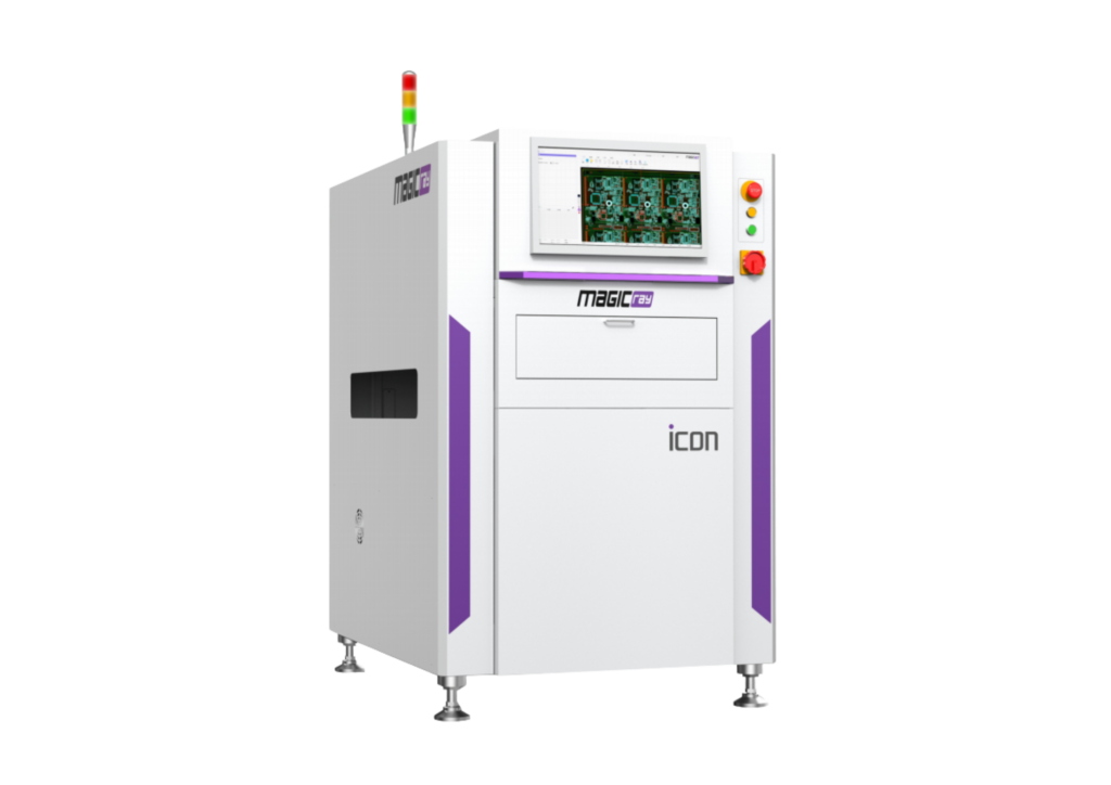
How SPI Works
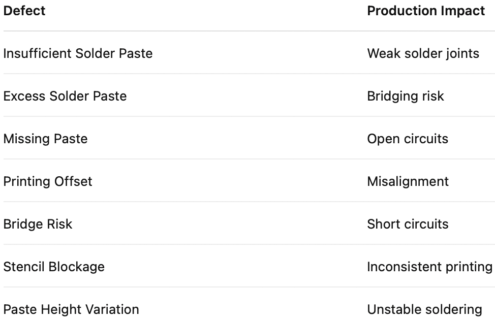
Modern SPI systems use advanced 3D optical measurement technology to analyze solder paste deposits.
SPI machines measure:
- Solder paste volume
- Solder paste height
- Solder paste area
- Printing offset
- Bridge risk
- Stencil blockage
The system compares measured values against predefined specifications and immediately identifies abnormalities.
Many modern SPI systems can also provide real-time feedback to solder paste printers, creating a closed-loop process control system.
Benefits of SPI Inspection
Early Defect Prevention
SPI identifies problems before components are mounted.
This prevents defective boards from moving further down the production line.
Improved First Pass Yield
Consistent solder paste deposition leads to more reliable solder joints.
Reduced Rework Costs
Defects found before placement are significantly cheaper to correct.
Better Process Control
SPI provides valuable data that helps optimize stencil printing performance.
Lower Scrap Rate
Preventing defects early minimizes wasted materials and production time.
What Is AOI Inspection?
Definition of AOI
AOI stands for Automatic Optical Inspection.
AOI systems inspect assembled PCBs after component placement and soldering.
The primary purpose of AOI is to verify the quality of the finished assembly.
Position in the SMT Process
Printer
↓
SPI
↓
Placement
↓
Reflow Oven
↓
AOI Inspection
↓
Testing
AOI serves as the final visual quality checkpoint before functional testing.
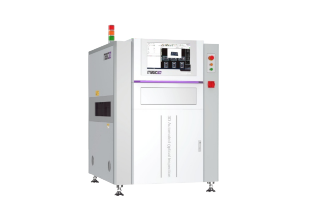
How AOI Works
AOI systems use:
- High-resolution cameras
- Multi-angle imaging
- Image comparison algorithms
- AI-assisted defect recognition
The system compares captured PCB images against reference data.
Common Defects Detected by AOI
- Missing components
- Incorrect components
- Component polarity errors
- Misalignment
- Tombstoning
- Lifted leads
- Solder bridges
- Insufficient solder joints
Modern AOI systems can inspect thousands of components within seconds.
Benefits of AOI Inspection
Detects Assembly Defects
AOI identifies problems that occur during placement and soldering.
Reduces Manual Inspection
Automated inspection improves consistency and reduces labor costs.
Improves Product Reliability
Defective products are detected before shipment.
Supports Traceability
Inspection results can be stored and linked to MES systems.
Enables Smart Manufacturing
AOI data supports continuous process improvement initiatives.
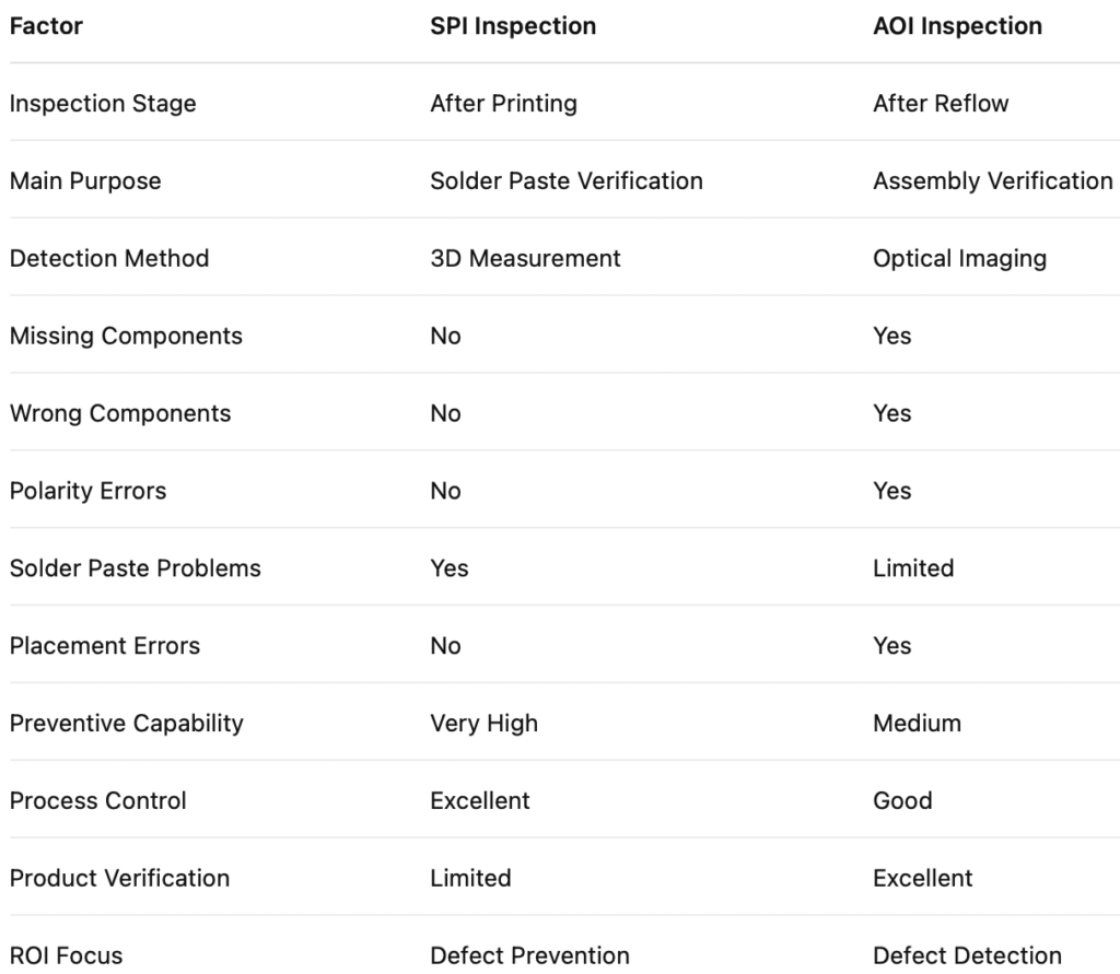
AOI vs SPI Inspection: Key Differences
Which Defects Can SPI Detect?
SPI focuses entirely on solder paste quality.
Since over 60% of SMT defects originate from printing issues, SPI plays a crucial role in defect prevention.
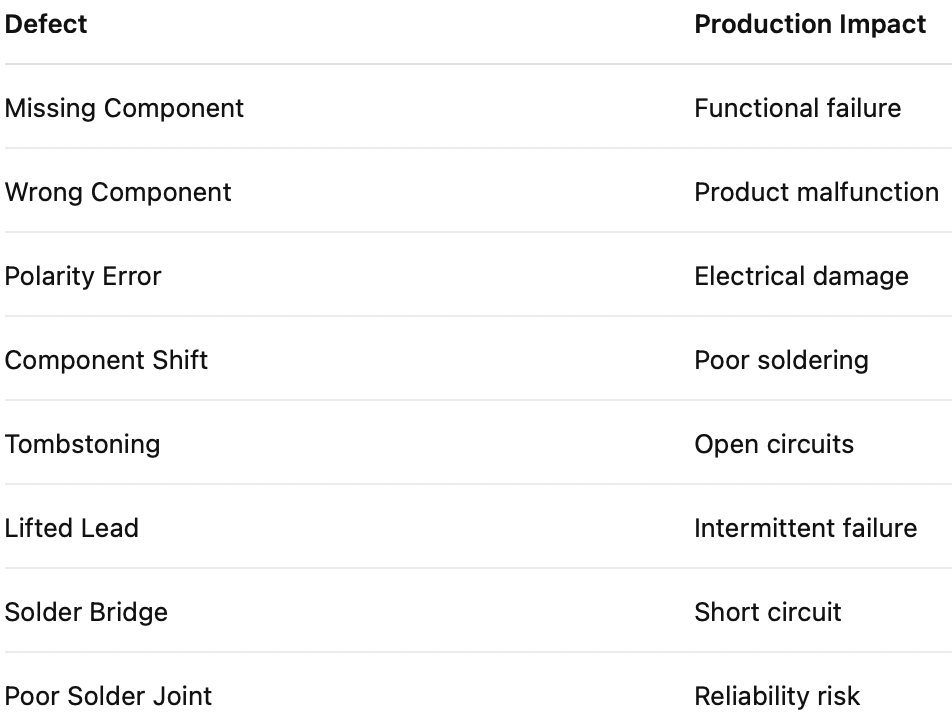
Which Defects Can AOI Detect?
AOI verifies overall assembly quality after soldering is completed.
AOI and SPI: Which Is More Important?
Many manufacturers ask:
Should I invest in AOI or SPI first?
This is often the wrong question.
SPI Prevents Defects
SPI identifies printing problems before assembly begins.
AOI Finds Defects
AOI identifies defects after they have already occurred.
SPI prevents waste.
AOI catches what SPI cannot.
The most effective SMT lines use both systems together.
AOI and SPI in Modern SMT Production Lines
Typical Inspection Workflow
PCB Loader
↓
Printer
↓
SPI
↓
Pick and Place
↓
Reflow Oven
↓
AOI
↓
Functional Test
↓
Packaging
This inspection strategy maximizes yield while minimizing rework costs.
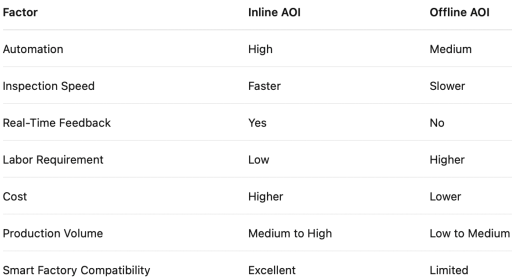
Inline AOI vs Offline AOI
Recommendation
Inline AOI
Suitable for:
- EMS factories
- Automotive electronics
- High-volume production
Offline AOI
Suitable for:
- Startups
- Small-batch production
- Budget-sensitive projects
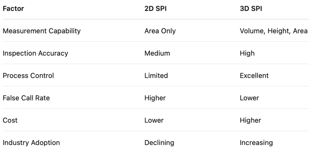
2D SPI vs 3D SPI
Why 3D SPI Is Becoming the Standard
As component sizes shrink to 0201 and 01005 packages, accurate volume measurement becomes increasingly important.
Most new SMT factories now prefer 3D SPI systems.
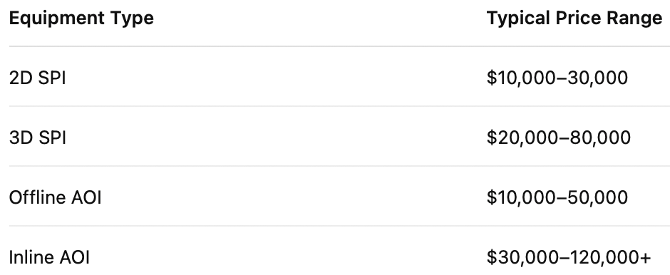
Cost Comparison: AOI vs SPI Systems
Although SPI adds upfront investment, it often delivers faster ROI by preventing defects before assembly.
Common Inspection Strategy Mistakes
Skipping SPI to Save Cost
Result:
Higher soldering defect rates.
Relying Only on AOI
Result:
Defects detected too late.
Choosing Systems Based Only on Price
Result:
Higher long-term operating costs.
Ignoring Data Analytics
Result:
Missed opportunities for process optimization.
Industry-Specific Recommendations
Consumer Electronics
Recommended:
SPI + Inline AOI
Automotive Electronics
Recommended:
3D SPI + Inline AOI + Full Traceability
Medical Devices
Recommended:
Complete inspection workflow with strict quality documentation.
LED Manufacturing
Recommended:
Cost-effective SPI + AOI combination.
Industrial Electronics
Recommended:
Flexible inspection systems with MES integration.
Why AOI and SPI Are Essential for Smart Factories
Modern Industry 4.0 manufacturing relies heavily on data-driven quality management.
AOI and SPI systems provide:
- Real-time process monitoring
- Defect trend analysis
- MES integration
- Quality traceability
- Predictive process control
These capabilities help manufacturers improve yield while reducing production costs.
Conclusion
When comparing AOI vs SPI inspection, there is no single winner.
SPI and AOI perform different but complementary functions.
- SPI prevents defects before assembly
- AOI detects defects after soldering
- SPI improves process control
- AOI verifies final product quality
For manufacturers seeking higher yields, lower rework costs, and improved product reliability, implementing both SPI and AOI inspection systems is the most effective strategy.
Before investing in SMT inspection equipment, companies should evaluate their production volume, quality requirements, automation goals, and long-term manufacturing plans.
Why Choose FULIU Electronics?
FULIU Electronics provides complete PCB assembly manufacturing solutions for customers worldwide, including:
- Turnkey SMT production line solutions
- AOI inspection systems
- SPI inspection systems
- SMT factory planning
- Production line layout design
- Reflow soldering equipment
- Installation and operator training
- Global delivery and technical support
Our team helps electronics manufacturers improve PCB assembly quality, reduce SMT defects, and maximize production efficiency through optimized inspection and manufacturing solutions.
Pingback: What Is Industrial PCBA? A Complete Guide for Manufacturers - Turnkey PCBA Line Solutions|Fuliu Electronics